

Capacitive sensor
A capacitive sensor and moving electrode technology, which is applied to instruments, measuring devices, measuring acceleration, etc., can solve the problem of difficulty in forming enhanced detection sensitivity, and achieve the effect of reducing sensitivity, uniform cross-sectional shape, and enhancing sensitivity.
- Summary
- Abstract
- Description
- Claims
- Application Information
AI Technical Summary
Problems solved by technology
Method used
Image

Examples
no. 1 example
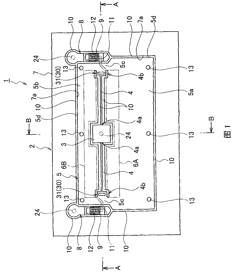
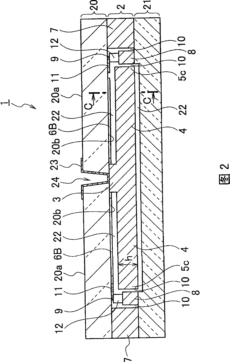
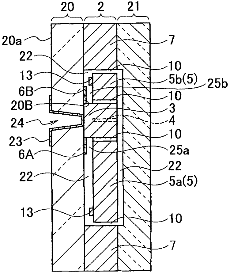
[0037] Such as figure 2 As shown, a capacitive sensor 1 (hereinafter, simply referred to as sensor 1) as a first embodiment of the present invention has a semiconductor layer 2 obtained by processing a semiconductor substrate, while insulating layers 20 and 21 such as a glass substrate are bonded by anodic bonding ( anodic bonding) on the front and rear sides, relatively shallow recessed portion 22 is formed in the bonding surface between the semiconductor layer 2 and the insulating layers 20 and 21, ensuring the insulating properties of the semiconductor layer 2 and the movable electrode 5 Ease of movement. In this embodiment, the bonding surface between the semiconductor layer 2 and the insulating layer 20 is provided with the recessed portion 22 on the side of the semiconductor layer 2, and the bonding surface between the semiconductor layer 2 and the semiconductor layer 2 is provided with the concave portion 22 on the semiconductor layer 2 side. The recessed portion 22...
no. 2 example
[0069] The sensor 1 as the second embodiment of the present invention differs from the first embodiment in the structure of the sensor 1 in that beam portions 4 and 4 are not provided at longitudinal ends such as Figure 9 The stress adjustment unit 30 is shown. In the second embodiment, as Figure 10 As shown in (a), the semiconductor layer 2 is bonded to the insulating layer 20, and before the gap 10 is formed, the recessed portion 22 is formed by various etching processes such as wet etching and dry etching. After cutting the semiconductor layer 2 by etching, the insulating layer 20 as the glass substrate is as Figure 10 The connection shown in (b) is processed by vertical etching, so as to form the Figure 10 Gap 10 shown in (c). After the recessed portion 22 is formed by an etching process, the stopper 13 is formed of an oxide film or an aluminum alloy.
[0070] By etching the semiconductor layer 2 which is the single crystal silicon substrate in this way, the recess...
no. 3 example
[0095] Second, will refer to Figure 17 and Figure 18 The structure of the sensor 1 as the third embodiment of the present invention will be described. In addition to the sensor 1 shown in the third embodiment can detect the physical value in the horizontal direction in the plane direction of the semiconductor layer 2, the sensor 1 shown in the third embodiment can detect the physical value in the vertical direction in the thickness direction of the semiconductor layer 2 The physical values shown in the second embodiment are the same as for sensor 1.
[0096] Figure 17 is a plan view showing the semiconductor layer 2 of the sensor 1 . Such as Figure 17 As shown, the semiconductor layer 2 includes: a vertical direction detection unit 50A for detecting a physical value in the vertical direction by forming a gap 10 in the semiconductor substrate through a known processing technology, a horizontal direction detection unit 50B for detecting a physical value in the horizont...
PUM
 Abstract
Description
Claims
Application Information