Method for manufacturing plane surface medium resistance discharging light source

A technology of dielectric barrier discharge and manufacturing method, applied in the field of electric vacuum, can solve the problems of uneven thickness and complicated process, and achieve the effect of simple and accurate manufacturing process and reduction of printing times.

Inactive Publication Date: 2010-06-02
IRICO
View PDF6 Cites 0 Cited by
  • Summary
  • Abstract
  • Description
  • Claims
  • Application Information

AI Technical Summary

Problems solved by technology

[0004] Aiming at the technical problems of the existing technology in the processing of the upper and lower substrates of the planar dielectric barrier discharge light source that require multiple printings and drying, the process is cumbersome and the thickness is uneven, the present invention proposes the following technical solutions:

Method used


Image

  • Method for manufacturing plane surface medium resistance discharging light source
  • Method for manufacturing plane surface medium resistance discharging light source
  • Method for manufacturing plane surface medium resistance discharging light source

Examples


Embodiment 1

[0030] a. Fabrication of the lower glass substrate 1:

[0031] 1) Use 2g of decontamination powder, analytically pure alcohol, and deionized water to perform ultrasonic cleaning on the glass substrate. There is no strict ratio requirement for alcohol and deionized water. After cleaning, the glass surface does not leave oil stains or stains, and the surface is smooth. The water film is required to be intact.

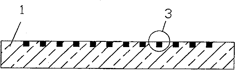
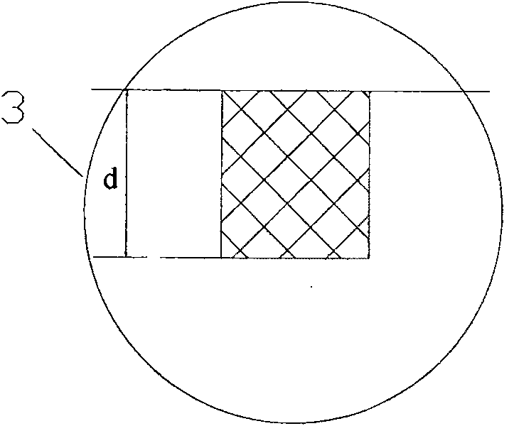
[0032] 2) On the lower glass substrate 1 glass, coat a layer of photosensitive glue with a thickness of 20 microns to resist the corrosion of glass etching solution, expose and develop through a mask plate, and form an electrode pattern, as shown in the attached image 3 shown;

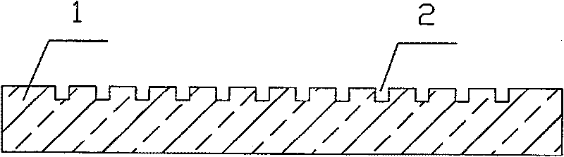
[0033] 3) Etching the lower substrate glass with a mixture of 40% hydrofluoric acid and pure water in a weight ratio of 4:1, and then peeling off the remaining photosensitive adhesive with a degumming solution, forming a and Groove 2 with consistent electrode pattern, as attached figure 1 show...

Embodiment 2

[0048] a. Fabrication of the lower glass substrate 1:

[0049] 1) Use 2 g of decontamination powder, analytically pure alcohol, and deionized water in sequence to ultrasonically clean the lower glass substrate.

[0050] 2) Coating a layer of 30 micron-thick photosensitive glue resistant to corrosion by glass etching solution on the glass of the lower glass substrate 1, exposing and developing through a mask to form an electrode pattern;

[0051] 3) Etching the glass of the lower glass substrate 1 with a mixture of 40% hydrofluoric acid and pure water in a weight ratio of 4:1, and then peeling off the remaining photosensitive adhesive with a degumming solution to form a Groove 2 consistent with the electrode pattern;

[0052] 4) After aligning the screen plate with the electrode pattern and the etched lower glass substrate with the “cross” alignment code, print the electrode in the groove 2 of the etched lower glass substrate, and place the printed electrode The lower glass s...

Embodiment 3

[0066] a. Fabrication of the lower glass substrate 1:

[0067] 1) Use 2 g of decontamination powder, analytically pure alcohol, and deionized water in sequence to ultrasonically clean the lower glass substrate.

[0068] 2) Coating a layer of 25 micron-thick photosensitive glue resistant to corrosion by glass etching solution on the glass of the lower glass substrate 1, exposing and developing through a mask to form an electrode pattern.

[0069] 3) Etching the lower glass substrate 1 glass with a mixture of 40% hydrofluoric acid and pure water in a weight ratio of 4:1, then peeling off the remaining photosensitive adhesive with a degumming solution, and placing it on the lower glass substrate A groove 2 consistent with the electrode pattern is formed;

[0070] 4) After aligning the screen plate with the electrode pattern and the etched lower glass substrate with the “cross” alignment code, print the electrode in the groove 2 of the etched glass substrate, and place the printe...


PUM

PropertyMeasurementUnit
thicknessaaaaaaaaaa
thicknessaaaaaaaaaa
thicknessaaaaaaaaaa

Abstract

The invention belongs to the electrovacuum field, and relates to a method for manufacturing a plane surface medium resistance discharging light source. The invention is characterized in that an electrode is printed and sintered in glass groove of an etched lower glass substrate, and then a reflecting layer and a medium layer are printed on the lower glass substrate. Particularly, the method comprises the following steps: a, the manufacture of the lower glass substrate, that is, applying photosensitive glue to the lower substrate glass to form an electrode pattern, subjecting the lower glass substrate to the etching treatment to form a groove which is consistent with the electrode pattern on the lower glass substrate, and subjecting the reflecting layer and the medium layer to printing a plurality of times after the sintering treatment; b, the manufacture of an upper substrate, that is, subjecting the upper glass substrate to ultrasonic cleaning and printing a fluorescent coating on theupper substrate; and c, encapsulating the whole machine, performing the low glass sintering, removing gas and then adding inertia mixed gas including neon and xenon, assembling a drive circuit and aging. The invention has the advantages of reducing the printing frequency of the medium and errors due to contrapostion, and ensuring that the manufacture technology is simple and accurate.

Description

technical field [0001] The invention belongs to the field of electric vacuum and relates to a method for manufacturing a planar dielectric barrier discharge light source. Background technique [0002] (1) In recent years, liquid crystal display LCD technology has achieved rapid development. Liquid crystal displays are generally transmissive, requiring a light source behind the liquid crystal panel to realize luminescent display. Important performance indicators such as brightness, contrast ratio, brightness uniformity and power consumption of LCD have a great relationship with the performance of its backlight source. At present, the backlight commonly used in flat-panel liquid crystal displays is cold-cathode fluorescent lamp CCFL, which has the advantages of high light efficiency and brightness, but its disadvantages are that it takes a long time to reach saturated brightness after lighting, the ignition is greatly affected by the ambient temperature and the life is short....

Claims


Application Information

Patent Timeline
Patent Type & Authority Patents(China)
IPC IPC(8): H01J9/00
Inventor 李军
Owner IRICO
Why Eureka
Try Eureka