Metal carrier band for packaging noncontact module with large size

A module packaging, non-contact technology, applied in the direction of electrical components, electrical solid devices, circuits, etc., can solve the problems of changing the production process, large-scale promotion and application difficulties, and achieve the effect of good application prospects

Inactive Publication Date: 2009-06-03
SHANGHAI CHANGFENG SMART CARD
View PDF0 Cites 5 Cited by
  • Summary
  • Abstract
  • Description
  • Claims
  • Application Information

AI Technical Summary

Problems solved by technology

However, with the continuous improvement of product requirements, many chips can no longer be packaged with traditional processes and materials.
[0003] Some people abroad have tried to change the standard and increase the size of the package body and module to realize the packaging of large-size chips, which alleviates the application of such large-size chips to a certain extent, but this method has changed most of the production process and requires A lot of money has been invested in the transformation of equipment and the production of new molds
It is more difficult to obtain mass promotion and application

Method used


Image

  • Metal carrier band for packaging noncontact module with large size
  • Metal carrier band for packaging noncontact module with large size
  • Metal carrier band for packaging noncontact module with large size

Examples


Embodiment Construction

[0030] In order to make the technical means, creative features, goals and effects achieved by the present invention easy to understand, the present invention will be further elaborated below in conjunction with specific examples.

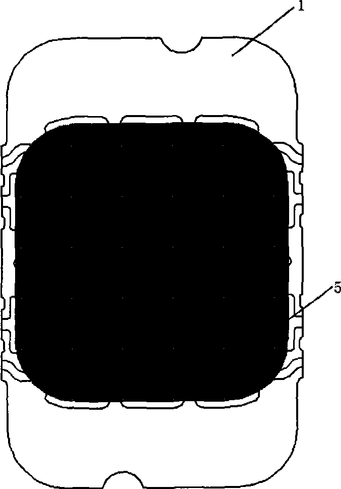
[0031] see Figure 14 , the tape base of the metal carrier tape for large-size non-contact module packaging of the present invention is prepared from copper or copper alloy materials, and constitutes the metal carrier tape 1 for module packaging, with a thickness of 0.06mm to 0.09mm; the thickness of the finished product is 0.065mm to 0.095mm. The appearance of the carrier tape 1 is formed by precision stamping.

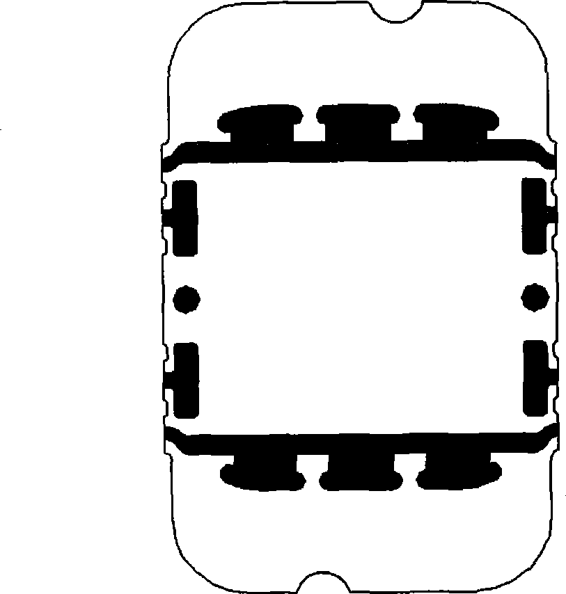
[0032] see Figure 4 , The chip carrying area 2 in the middle of the metal carrier tape 1 is realized by a precision stamping process. The chip carrying area 2 can carry a 3.9*4.5mm size chip to meet the requirements of large-sized non-contact products such as electronic passports and financial cards.

[0033] see Figure 4 , Figure ...


PUM


Abstract

The invention provides a metal carrier band for packaging a noncontact module with large size which is characterized in that the metal carrier band comprises a chip bearing region which can bear a chip of 3.9*4.5mm. The chip which is 1.5 times of the area of a common chip can be bear and packaged, and a module product with the same mechanical size is obtained. By the improvement of the metal carrier band and under the premise of the increased size of the packaged chip, the combining force of a mould body with the metal carrier band is improved to the maximum extent after the mould packaging, therefore, the mechanical force resistance of internal devices is improved greatly. The carrier band is packaged in a reeling way. Under the premise of not adding the investment, the present conventional packaging process and the existing equipment can be used for producing products with better quality, therefore, the application of high-end chips, such as noncontact intelligent electronic passport, EMV band card, and the like in the intelligent card field is expanded.

Description

technical field [0001] The invention relates to the technical field of microelectronic semiconductor packaging, in particular to the technical field of non-contact smart card module packaging. In particular, it is a metal carrier tape for large-size non-contact module packaging. Background technique [0002] With the continuous improvement of integrated circuit packaging technology, the integration level of integrated circuits is increasing day by day, and the functions are becoming more and more abundant. It is required to accommodate larger chips in a relatively small package size. Under the premise that the size and thickness of integrated circuit products remain unchanged, the packaging of some chips has reached the limit of packaging equipment and technology. For example, the current traditional contactless smart card modules used for contactless cards (such as public transportation cards, China's second-generation ID cards and most other applications) have an external...

Claims


Application Information

Patent Timeline
Patent Type & Authority Applications(China)
IPC IPC(8): H01L23/13H01L23/488
CPCH01L2924/0002
Inventor 杨辉峰顾秋华
Owner SHANGHAI CHANGFENG SMART CARD
Why Eureka
Try Eureka