Package structure and manufacturing method thereof

A technology of packaging structure and manufacturing method, which is applied in the direction of semiconductor/solid-state device manufacturing, semiconductor/solid-state device components, semiconductor devices, etc., to achieve the effect of optimizing cost

Inactive Publication Date: 2019-07-05
POWERTECH TECHNOLOGY INC
View PDF6 Cites 0 Cited by
  • Summary
  • Abstract
  • Description
  • Claims
  • Application Information

AI Technical Summary

Problems solved by technology

Therefore, how to use existing equipment to complete the processing steps to minimize equipment cost and overall manufacturing cost has become a challenge for researchers in this field.

Method used


Image

  • Package structure and manufacturing method thereof
  • Package structure and manufacturing method thereof
  • Package structure and manufacturing method thereof

Examples


Embodiment Construction

[0024] Reference will now be made in detail to the exemplary embodiments of the present invention, examples of which are illustrated in the accompanying drawings. Wherever possible, the same reference numbers will be used in the drawings and description to refer to the same or like parts.

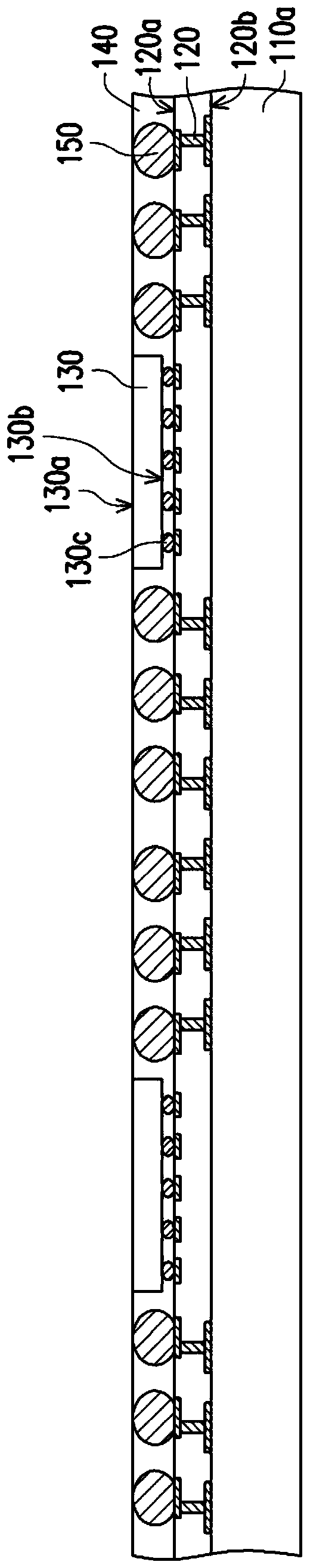
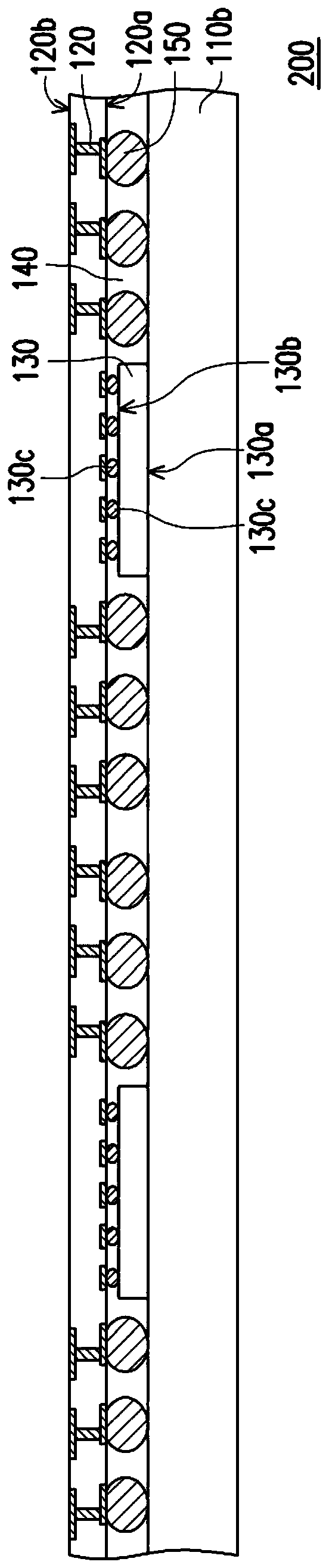
[0025] figure 1 is a schematic cross-sectional view of a manufacturing method of a packaging structure according to an embodiment of the present invention. Please refer to figure 1 , figure 1 Only a portion of the package structure at an intermediate stage of the manufacturing process is shown. A plurality of redistribution circuit patterns 120 are formed on the carrier 110a. The carrier 110a is, for example, a glass substrate or other suitable substrate material, as long as the substrate material can withstand subsequent processes of the package structure formed thereon, the invention is not limited thereto. The redistribution pattern 120 includes a first surface 120a and a second sur...


PUM


Abstract

The invention provides a package structure and a manufacturing method thereof. The method includes at least the following steps. A package panel is provided. The package panel includes a first encapsulation, a plurality of first integrated circuit components and a plurality of redistribution circuit patterns electrically connected to the first integrated circuit components, the first integrated circuit components are encapsulated by the first encapsulation, and the redistribution circuit patterns are distributed on the first encapsulation and the first integrated circuit components. The firstencapsulation of the package panel is cut to form a plurality of singulated package strips. One of the singulated package strips is attached onto an attachment region of a substrate. The substrate includes at least one positioning hole distributed outside of the attachment region. The package process is performed over the singulated package strip with the substrate affixed through the positioninghole to form the package structure.

Description

technical field [0001] The invention relates to a manufacturing method, in particular to a packaging structure and a manufacturing method thereof. Background technique [0002] In general, wafer-level or panel-level packaging should be understood to include performing the entire package, interconnect structure, and other process steps on a wafer, such as wire bonding, Die bonding or molding process. However, performing such wafer-level or panel-level processes requires large-scale equipment. Furthermore, such large-scale equipment requires a very large capital investment, which is not cost-effective. Therefore, how to use existing equipment to complete the processing steps to minimize the equipment cost and the overall manufacturing cost has become a challenge for researchers in this field. Contents of the invention [0003] The invention provides a manufacturing method of a packaging structure, which can increase the yield and provide process stability. [0004] The i...

Claims


Application Information

Patent Timeline
Patent Type & Authority Applications(China)
IPC IPC(8): H01L21/60H01L23/488H01L23/49
CPCH01L24/83H01L24/85H01L24/97H01L24/48H01L24/49H01L24/32H01L2224/83005H01L2224/85005H01L2224/97H01L2224/32227H01L2224/48091H01L2224/48149H01L2224/48159H01L2224/49052H01L2224/49175H01L24/73H01L25/0657H01L2224/32145H01L2224/32225H01L2224/48145H01L2224/73265H01L2224/81005H01L2225/0651H01L2225/06517H01L2924/1433H01L2924/15311H01L2924/1533H01L2924/18161H01L2924/19041H01L2924/19042H01L2924/19043H01L2225/06506H01L2225/06562H01L23/3128H01L21/568H01L21/6835H01L25/18H01L21/561H01L25/50H01L2221/68309H01L2224/48227H01L24/16H01L2224/16227H01L2924/19105H01L23/49827H01L23/49816H01L2224/81H01L2924/00012H01L2224/83H01L2224/85H01L2924/00H01L2221/68368H01L2924/19106
Inventor 锺馨德庄咏程林国鼎林南君
Owner POWERTECH TECHNOLOGY INC
Why Eureka
Try Eureka