

Etching method and dual damascene structure forming method
A technology of etching gas and etching time, used in electrical components, semiconductor/solid-state device manufacturing, circuits, etc., can solve problems such as uniformity and poor consistency, achieve uniform polymer distribution, improve uniformity, and improve etching quality effect
- Summary
- Abstract
- Description
- Claims
- Application Information
AI Technical Summary
Problems solved by technology
Method used
Image

Examples
no. 1 example
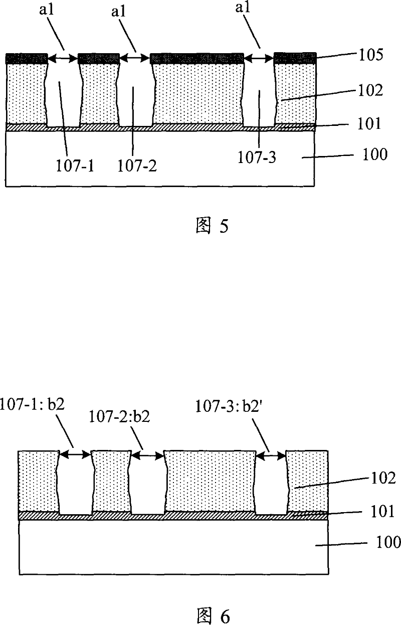
[0085] In this embodiment, through holes (or contact holes) are formed in the dielectric layer by using the etching method of the present invention.
[0086] Figure 7 It is a flow chart of the etching method in the first embodiment of the present invention, Figure 8 to Figure 12 In order to illustrate the device cross-sectional view of the etching method of the first embodiment of the present invention, below in conjunction with Figure 7 to Figure 12 The first embodiment of the present invention will be described in detail.
[0087] Step 701: Provide a substrate with a dielectric layer on the substrate.
[0088] The substrate in this embodiment may be a substrate on which metal-oxide-semiconductor transistors have been formed, or a substrate on which an underlying metal wiring structure has been formed (not shown in the figure).
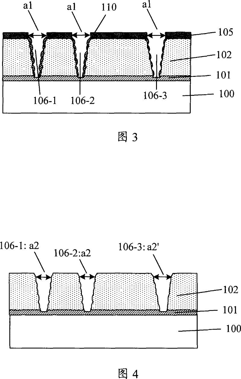
[0089] In addition, in order to improve the uniformity and consistency of the etching pattern in terms of etching depth, usually an etching st...
PUM
 Abstract
Description
Claims
Application Information