Mounting structure, electrooptic device, and electronic apparatus

An electro-optical device and structure technology, applied in the direction of fixed capacitor dielectric, printed circuit assembled with electrical components, printed circuit connected with non-printed electrical components, etc., can solve problems such as harsh noise, environmental deterioration, and downgrade of electronic equipment , achieve the effect of suppressing the increase of manufacturing cost and reducing noise

Inactive Publication Date: 2009-06-17
EPSON IMAGING DEVICES CORP
View PDF2 Cites 1 Cited by
  • Summary
  • Abstract
  • Description
  • Claims
  • Application Information

AI Technical Summary

Problems solved by technology

[0006] However, in electronic equipment having a wiring board on which electronic components are surface-mounted as described above, there is a problem that vibrations generated from the electronic components are transmitted to the wiring board to generate harsh noise, which disturbs the electronic equipment. Degradation, especially in the case of portable electronic devices such as mobile phones, will worsen the environment when carried
[0007] Moreover, in the structure described in the above-mentioned Patent Document 1, since the opening provided on the wiring board is limited to the outside of the corner of the electronic component, or is limited to the wiring board connected to the terminal of the electronic component, The outer side of the terminals on the side, so although it is effective in preventing damage to the terminals on the wiring board side, it has the problem that the above-mentioned noise generated from electronic components cannot be effectively reduced.
[0008] In addition, in the structure described in the above-mentioned Patent Document 2, since surface-mount electronic components cannot be directly mounted on the wiring board, it is considered that the advantages of surface mounting are lost, especially the thinning of the mounting structure and the mounting process. However, it has become an obstacle to realize the miniaturization and thinning of electronic equipment or the reduction of manufacturing cost in recent years.

Method used


Image

  • Mounting structure, electrooptic device, and electronic apparatus
  • Mounting structure, electrooptic device, and electronic apparatus
  • Mounting structure, electrooptic device, and electronic apparatus

Examples


Embodiment Construction

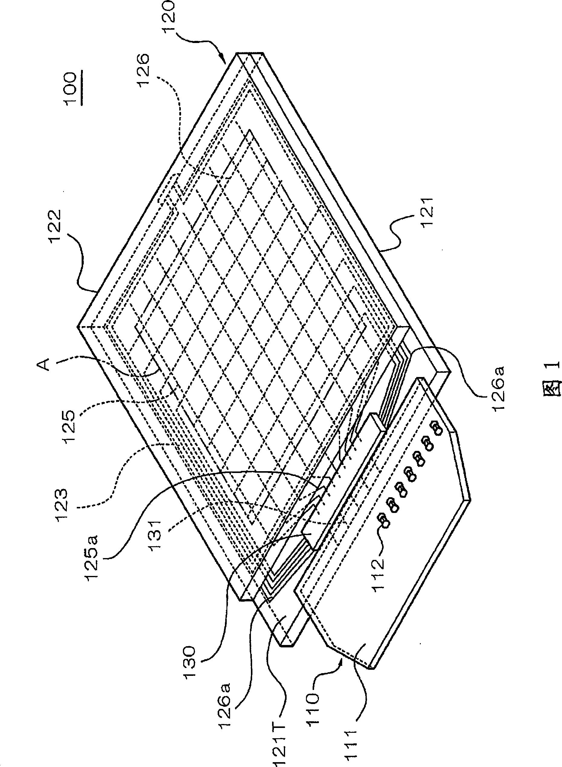
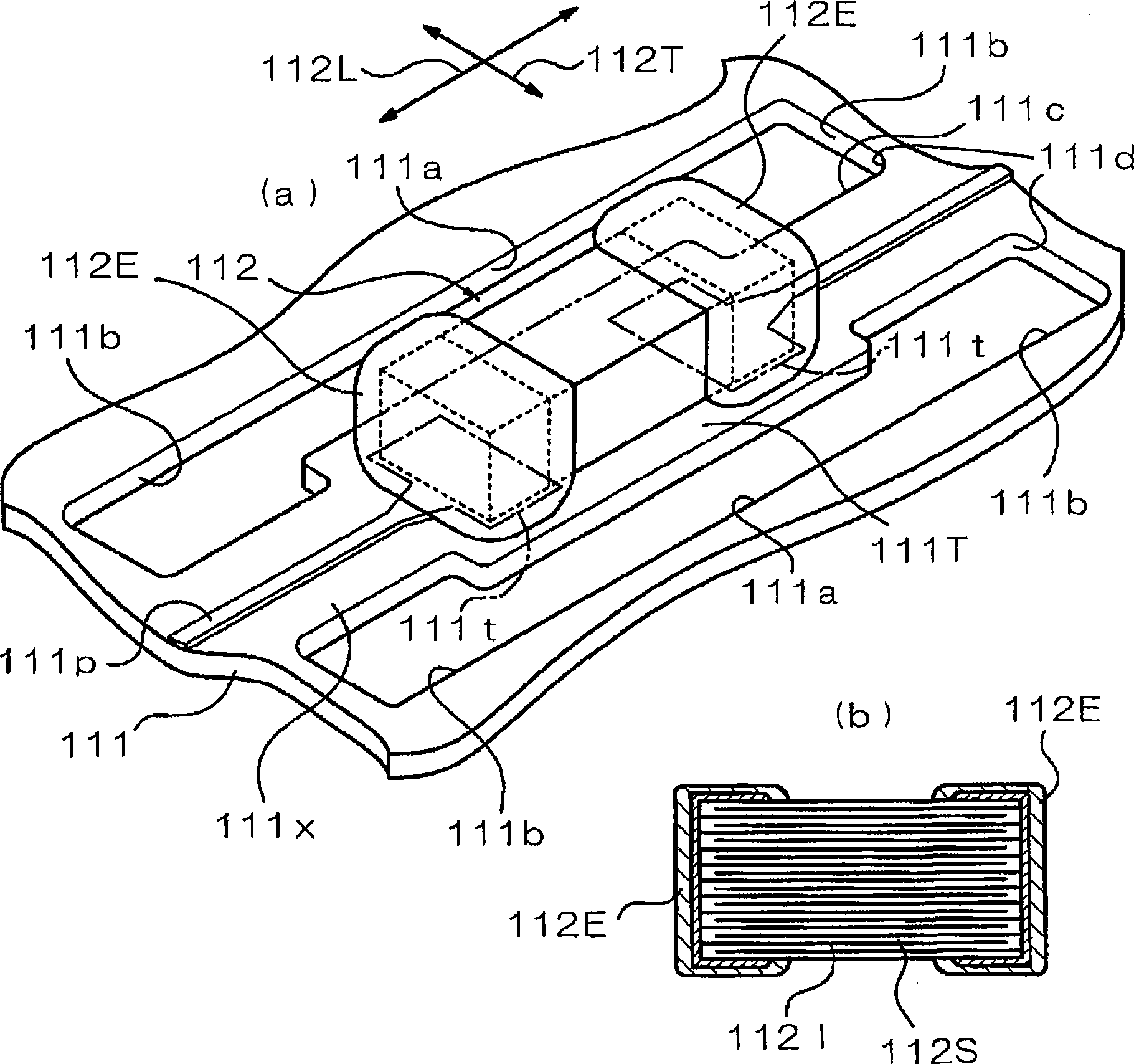
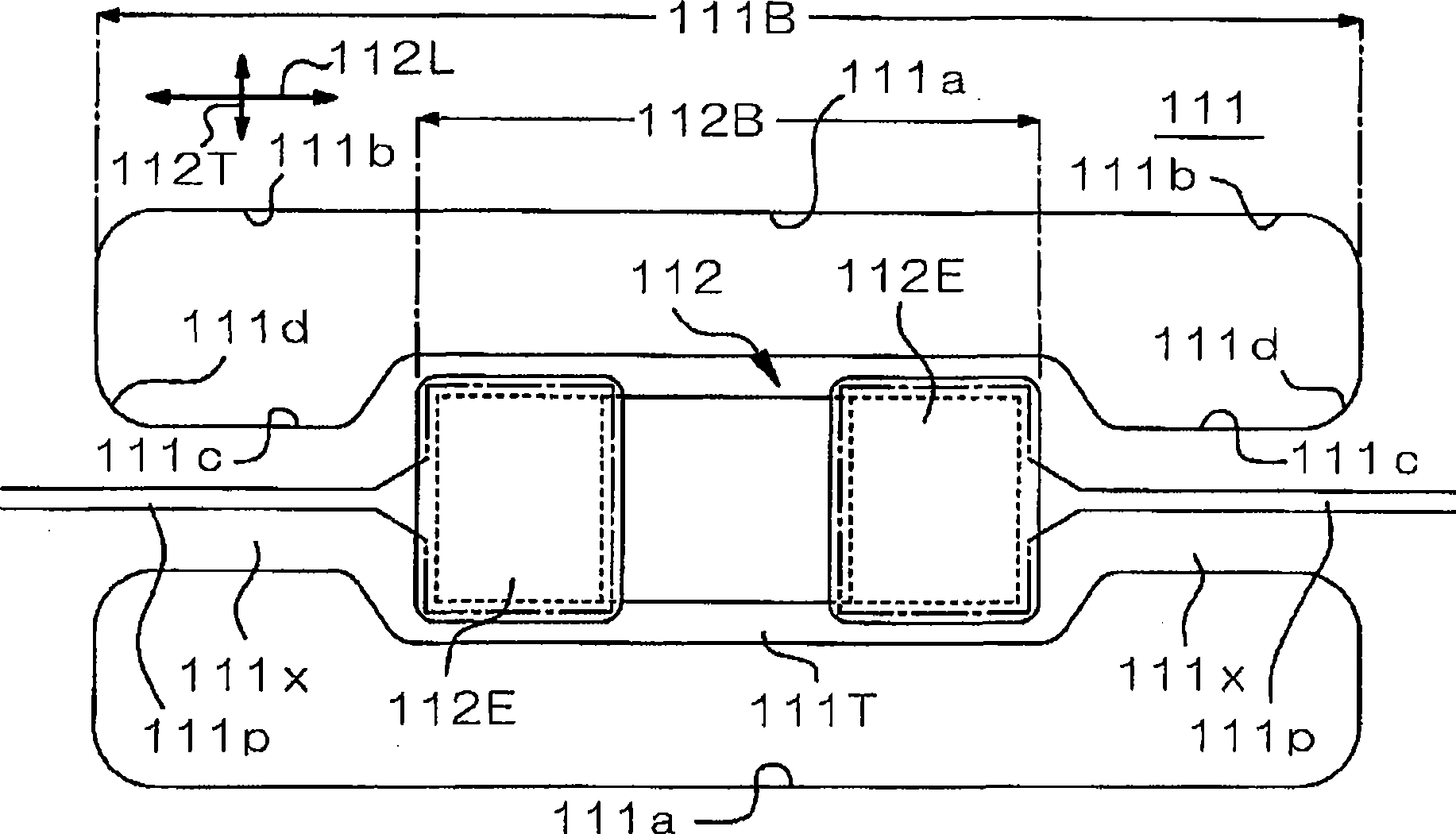
[0057] Next, embodiments of the present invention will be described in detail with reference to the drawings. FIG. 1 is a schematic perspective view showing a schematic structure of an electro-optical device 100 including a mounting structure as an embodiment of the present invention. The electro-optical device 100 of this embodiment includes a mounting structure 110. This mounting structure 110 is a mounting structure in which, for example, an electronic component 112 as a multilayer ceramic capacitor is mounted on a wiring board 111 made of a flexible wiring board. The wiring board 111 has: a plate-shaped resin base material made of an insulating resin material such as polyimide, and wiring not shown made of aluminum, copper, etc., formed on the surface of the resin base material; Equipped with surface resist, cover film, etc. covering these parts.

[0058] The electro-optical device 100 has an electro-optical panel 120 connected to the above-mentioned mounting structure 110. In...


PUM


Abstract

The invention realizes a structure of a mounting structure, an electro light device and an electronic device, wherein the mounting structure, the electro light device and the electronic device can effectively reduce the noise generated by the oscillation of an electronic element which is mounted on a wiring board. The mounting structure (100) of the invention is a mounting structure which mounts the electronic element (112) with a shape of longer direction (112L) on the wiring board (111), and is characterized by having an opening (111a) which is adjacent to an exterior surface extending in the longer direction (112L) in the exterior surface of a mounting region (111T) of the electronic element (112) and is arranged to at least extend all over the whole length range (112B) of the longer direction (112L) of the electronic element (112).

Description

Technical field [0001] The present invention relates to a mounting structure, an electro-optical device, and an electronic device, and more particularly to a mounting structure in which electronic components such as multilayer ceramic capacitors are mounted on a wiring board. Background technique [0002] Generally, mounting structures in which electronic components are mounted on wiring boards such as flexible wiring boards are arranged inside various electronic devices. In such mounting structures, as electronic components, most of them contain capacitors as components of electronic circuits. In particular, with the miniaturization and thinning of electronic devices in recent years, in order to achieve the miniaturization and manufacturing process of electronic components For automation, most of the small multilayer ceramic capacitors of the surface mount type are used. [0003] As a mounting structure for mounting minute electronic components on a wiring board as described abo...

Claims


Application Information

Patent Timeline
Patent Type & Authority Applications(China)
IPC IPC(8): H05K1/18G02F1/13
CPCH01G4/12H05K1/181H05K3/303H05K3/32
Inventor 古谷直祐小林伸一藤卷由贵
Owner EPSON IMAGING DEVICES CORP
Why Eureka
Try Eureka