Ceramic antenna structure

A ceramic antenna and carrier technology, applied in the structural form of the radiating element, antenna support/mounting device, etc., can solve the problems that the electronic device cannot receive or transmit signals, the ceramic antenna is separated from the circuit board, and the efficiency cannot be achieved.

Inactive Publication Date: 2009-06-24
SHENZHEN FUTAIHONG PRECISION IND CO LTD
View PDF0 Cites 2 Cited by
  • Summary
  • Abstract
  • Description
  • Claims
  • Application Information

AI Technical Summary

Problems solved by technology

Once the portable electronic device is accidentally dropped from a high place, it is easy to separate the ceramic antenna from the circuit board, resulting in the electronic device being unable to receive or transmit any signal
Moreover, the ceramic antenna cannot achieve the efficiency of -3dBi (that is, 50%) when the optimum frequency of the antenna is 2450MHz only by the radiating element 20, the grounding element 30 and the input element 40 printed on the carrier 10.

Method used


Image

  • Ceramic antenna structure
  • Ceramic antenna structure
  • Ceramic antenna structure

Examples


Embodiment Construction

[0050] The detailed description and technical content of the present invention are described below with accompanying drawings. However, the attached drawings are provided for reference and illustration only, and are not intended to limit the present invention.

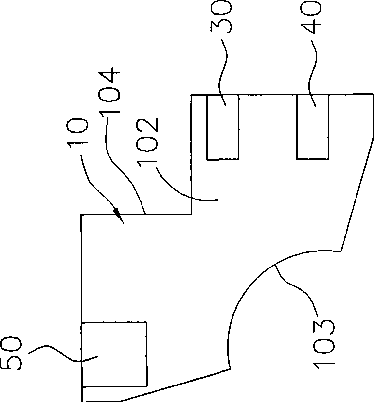
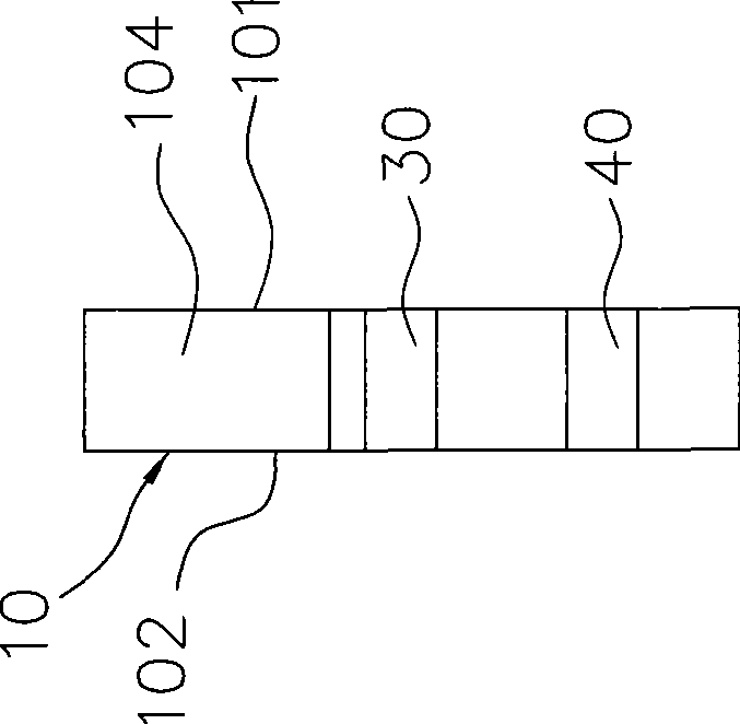
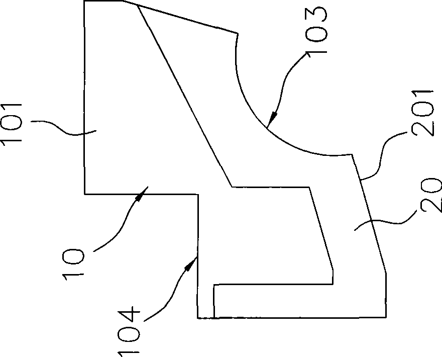
[0051] see Figure 2 to Figure 4 , is a schematic diagram of the appearance, decomposition and bottom view of the ceramic antenna structure in the present invention. The ceramic antenna structure in the present invention includes a carrier 1 , a radiation component 2 , a ground component 3 , an input component 4 and a fixing pin 5 .

[0052] The carrier 1 is made of a ceramic material with a dielectric coefficient of 19.4, has a first side 11 and a second side 12 on it, and a first end 13 and a second end 14 connected to the first and second sides 11, 12, The first end 13 has an arc-shaped notch 131 , and the second end 14 has an L-shaped notch 141 . In addition, a through hole 15 adjacent to the L-shaped notch 141 i...


PUM


Abstract

The invention discloses a ceramic antenna structure which is fixedly connected on a circuit board of a portable electronic device; the ceramic antenna structure comprises a carrier, a radiating element, a grounding element, an inputting element and a fixing needle; a first and a second side surfaces and a first end and a second end which are connected with the first side surface and the second side surface are arranged on the carrier. A penetrating hole is arranged on the carrier, and a first metal pattern is arranged at the position of the edge of the penetrating hole of the first side surface; the radiating element is attached on the first side surface of the carrier, and an outer edge part is arranged on the radiating element. The grounding element and the inputting element are electrically connected with the outer edge part of the radiating element at the connecting position of the first side surface and the second end and are extended to the second side surface. The fixing needle is arranged in the penetrating hole of the carrier in a penetrating way and is electrically connected with the first metal pattern. After the fixing needle penetrates through the penetrating hole, and the part of the fixing needle, penetrating out of the carrier, penetrates a through hole of the circuit board and is fixedly connected with the circuit board.

Description

technical field [0001] The present invention relates to an antenna, in particular to a ceramic antenna structure. Background technique [0002] With the vigorous development of wireless communication, many communication products tend to be miniaturized. In order to meet this requirement, some embedded antennas also require small size. At present, the commonly used tiny antennas include chip antennas and planar antennas, because these types of antennas are easy to achieve low height and small size, among which the most popular among chip antennas is low-temperature co-fired ceramics. Technology (LTCC) ceramic chip antenna (ceramic chip antenna). [0003] see Figure 1(a) to Figure 1(c) As shown, the ceramic antenna structure includes a carrier 10 , a radiation element 20 , a ground element 30 , an input element 40 and a fixed point 50 . The carrier 10 has a first side 101 and a second side 102, and a first end 103 and a second end 104 connected to the first and second sides...

Claims


Application Information

Patent Timeline
Patent Type & Authority Applications(China)
IPC IPC(8): H01Q1/38H01Q1/24
Inventor 黄韵芳
Owner SHENZHEN FUTAIHONG PRECISION IND CO LTD
Why Eureka
Try Eureka