Semiconductor device including a dopant blocking superlattice and associated methods

A semiconductor and dopant technology, applied in semiconductor devices, electrical components, circuits, etc., can solve problems such as device performance degradation

A semiconductor and dopant technology, applied in semiconductor devices, electrical components, circuits, etc., can solve problems such as device performance degradation

CN101467259AInactive Publication Date: 2009-06-24梅尔斯科技公司

Image

  • Semiconductor device including a dopant blocking superlattice and associated methods
  • Semiconductor device including a dopant blocking superlattice and associated methods
  • Semiconductor device including a dopant blocking superlattice and associated methods

Examples


Embodiment Construction

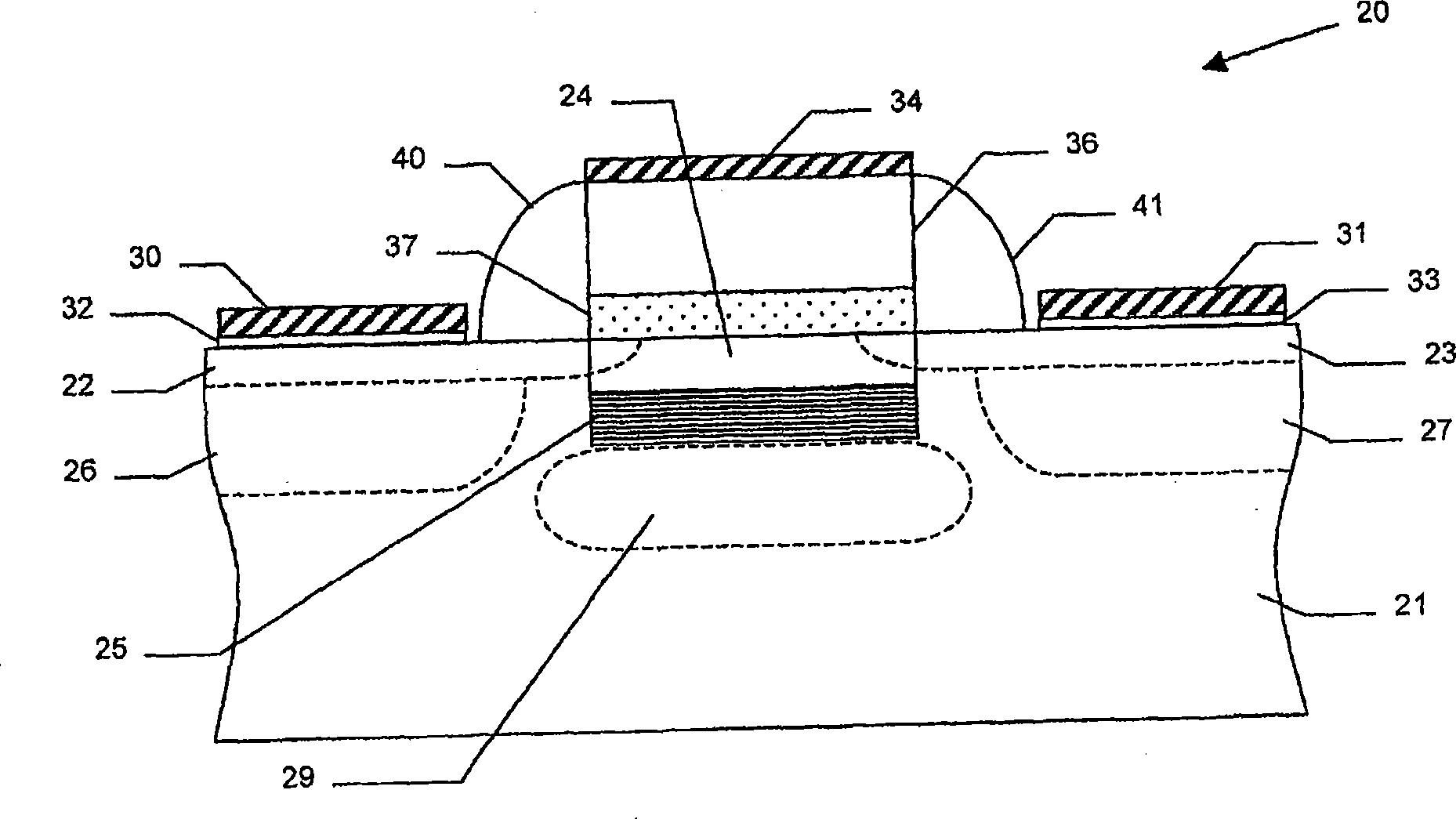
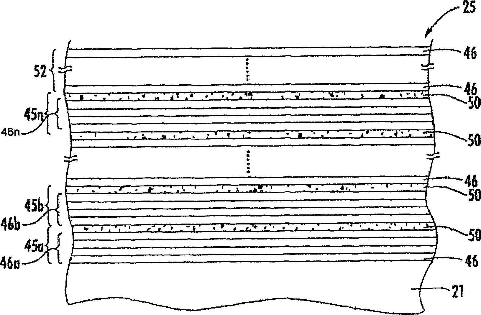
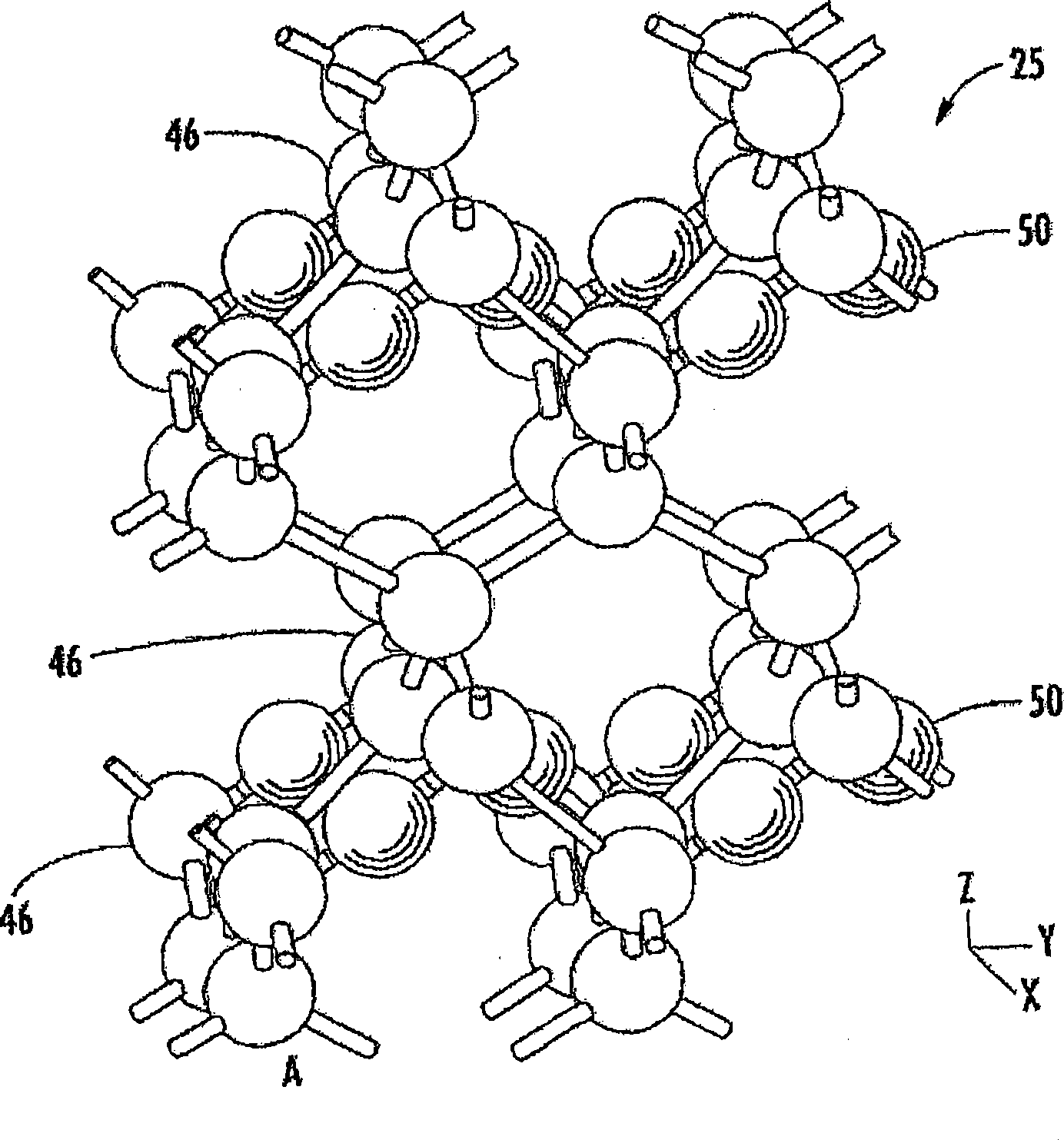
[0028] The present invention will be described more fully below with reference to the accompanying drawings, in which preferred embodiments of the present invention are shown. However, the present invention can be implemented in many different forms, and should not be considered limited to the embodiments set forth herein. On the contrary, these embodiments are provided to make this disclosure thorough and complete, and to fully convey the scope of the present invention to those skilled in the art. The same numbers always refer to the same elements, and the main numbers are used to refer to similar elements in alternative embodiments.

[0029]The present invention relates to controlling the properties of semiconductor materials at the atomic or molecular level to obtain improved performance in semiconductor devices. In addition, the present invention relates to the identification, production, and use of improved materials used in the conductive paths of semiconductor devices.

[0...


PUM


Abstract

A semiconductor device may include at least one metal oxide field-effect transistor (MOSFET). The at least one MOSFET may include a body, a channel layer adjacent the body, and a dopant blocking superlattice between the body and the channel layer. The dopant blocking superlattice may include a plurality of stacked groups of layers. Each group of layers of the dopant blocking superlattice may include a plurality of stacked base semiconductor monolayers defining a base semiconductor portion, and at least one non-semiconductor monolayer constrained within a crystal lattice of adjacent base semiconductor portions.

Description

Technical field [0001] The present invention relates to the field of semiconductors, and more specifically, to semiconductors with enhanced performance such as energy band engineering-based semiconductors and related methods. Background technique [0002] Various structures and techniques have been proposed to enhance the performance of semiconductor devices, such as by increasing the mobility of charge carriers. For example, US Patent Application 2003 / 0057416 by Currie et al. discloses strained material layers of silicon, silicon-germanium, and relaxed silicon, and also includes impurity-free regions that may additionally cause performance degradation. The resulting biaxial strain in the upper silicon layer changes the carrier mobility, enabling higher speed and / or lower power devices. Published US Patent Application 2003 / 0034529 by Fitzgerald et al. discloses CMOS inverters that are also based on similar strained silicon technology. [0003] Takagi's US Patent No. 6,472,685 B2 ...

Claims


Application Information

Patent Timeline
24 Jun 2009
Publication
CN101467259A
IPC
H01L29/10; H01L29/15
Inventors
M·伊萨; R·J·史蒂芬森