LED chip encapsulation method and construction having high efficient lateral direction light emission effect

A technology of chip packaging structure and light-emitting diodes, which is applied in the manufacture of electrical components, electrical solid devices, semiconductor/solid devices, etc., can solve problems such as inconvenience, loss, and inability to obtain heat dissipation effects, and achieve the effect of shortening the process time

Active Publication Date: 2009-07-08
HARVATEK CORPORATION
View PDF0 Cites 6 Cited by
  • Summary
  • Abstract
  • Description
  • Claims
  • Application Information

AI Technical Summary

Problems solved by technology

In other words, due to the fact that the length l1 of the base S1 is too short, the conventional LED chip D will not be able to obtain effective heat dissipation, and the LED chip D will burn out due to overheating.
[0005] Therefore, it can be seen from the above that the current packaging methods and packaging structures of light-emitting diodes obviously have inconveniences and shortcomings, and those that need to be improved

Method used


Image

  • LED chip encapsulation method and construction having high efficient lateral direction light emission effect
  • LED chip encapsulation method and construction having high efficient lateral direction light emission effect
  • LED chip encapsulation method and construction having high efficient lateral direction light emission effect

Examples


Embodiment Construction

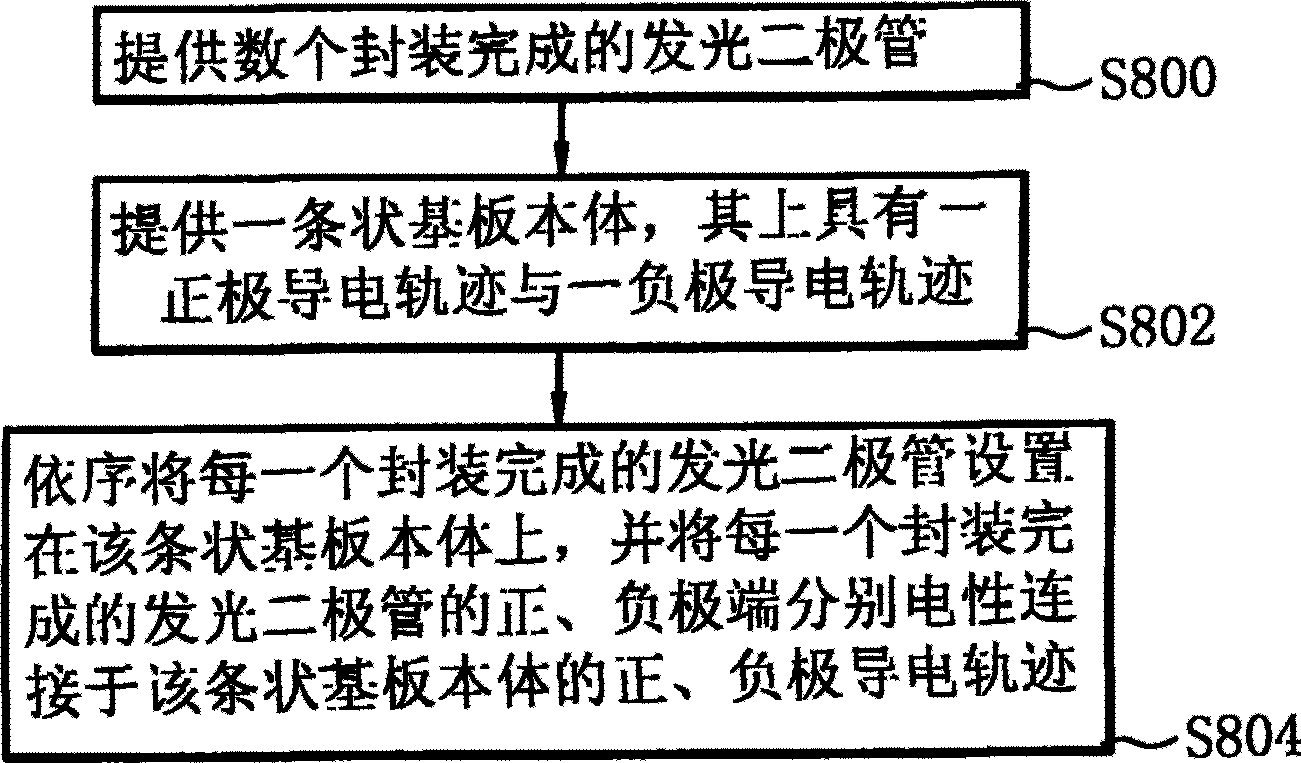
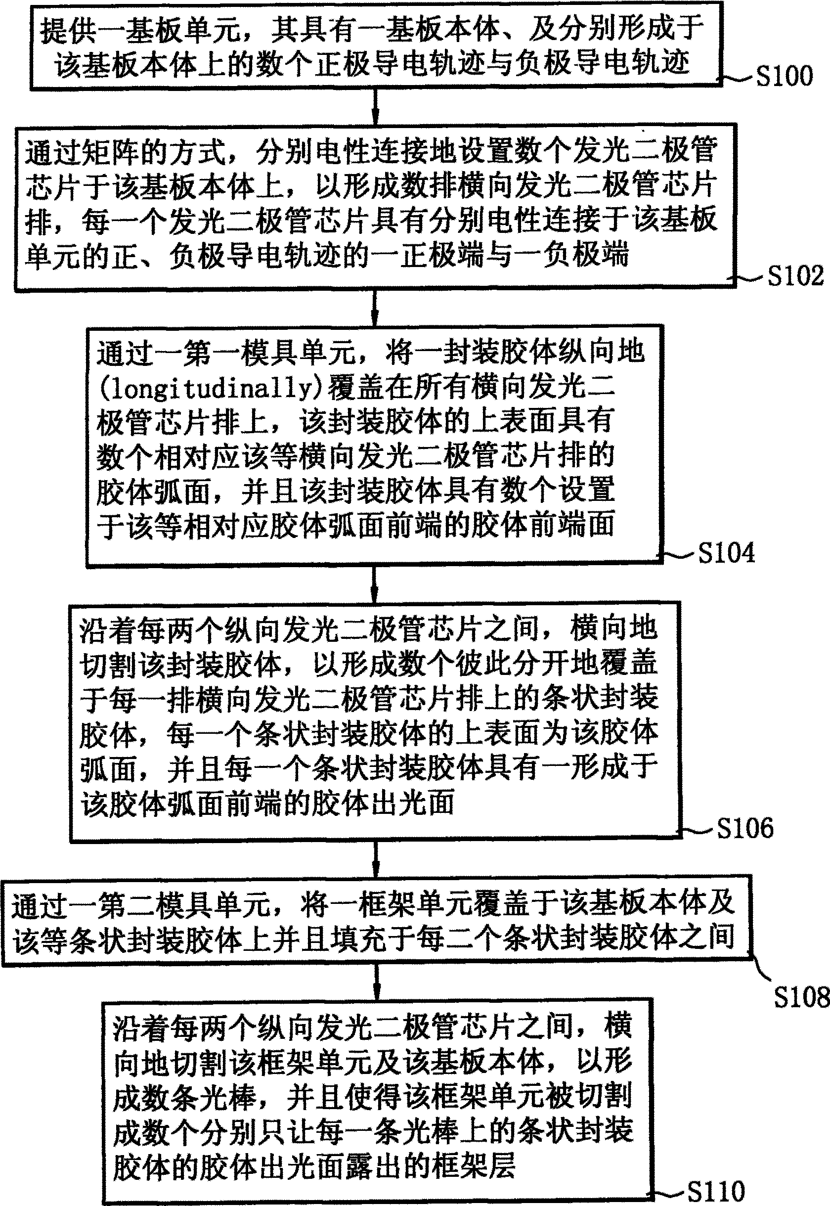
[0071] see image 3 , 3b e62d2c-ed59-4f8a-865a-c3064bbd105f, and Figure 3A to Figure 3F shown. image 3 It is a flow chart of the first embodiment of the packaging method of the present invention, Figure 3a to Figure 3d are respectively a schematic diagram of the packaging process of the first embodiment of the packaging structure of the present invention, Figure 3A to Figure 3D They are schematic cross-sectional views of the packaging process of the first embodiment of the packaging structure of the present invention. Depend on image 3 It can be seen from the flow chart that the first embodiment of the present invention provides a method for packaging a light-emitting diode chip with a high-efficiency lateral light-emitting effect, which includes the following steps:

[0072] First of all, please cooperate Figure 3a and Figure 3A As shown, a substrate unit 1 is provided, which has a substrate body (substrate body) 10, and several positive electrode traces (positi...


PUM


Abstract

The invention relates to a light-emitting diode chip packaging structure with high-efficiency lateral lighting effect. The structure comprises a base plate unit, a light-emitting unit, a package colloid unit and a frame unit, wherein, the light-emitting unit comprises a plurality of light-emitting diode chips which are electrically arranged on the base plate unit. The package colloid unit comprises a stripe package colloid covering the light-emitting diode chips, wherein, a colloid arc surface and a colloid light-exiting surface are arranged on the upper surface and the front surface of the stripe package colloid respectively. The frame unit adopts a frame layer covering the base plate unit and coating the stripe package colloid, and only the colloid light-exiting surface is exposed.

Description

technical field [0001] The present invention relates to a packaging method of a light-emitting diode chip and its packaging structure, in particular to a packaging method of a light-emitting diode chip with a high-efficiency lateral light-emitting effect (high-efficiency lateral light-emitting effect) and its packaging structure. Background technique [0002] see figure 1 As shown in FIG. 1 , it is a flow chart of an existing packaging method for light emitting diodes. It can be known from the flow chart that the steps of the existing LED packaging method include: firstly, providing several packaged LEDs (packaged LED) (S800); then, providing a stripped substrate body, on which There is a positive electrode trace (positive electrode trace) and a negative electrode trace (negative electrode trace) (S802); finally, each packaged light-emitting diode (packaged LED) is arranged on the strip substrate body in sequence, and The positive and negative terminals of each packaged LE...

Claims


Application Information

Patent Timeline
Patent Type & Authority Applications(China)
IPC IPC(8): H01L21/50H01L25/00H01L25/075H01L23/31
CPCH01L24/97H01L2224/48091H01L2924/12041H01L2924/15747H01L2924/1815
Inventor 汪秉龙巫世裕吴文逵
Owner HARVATEK CORPORATION
Why Eureka
Try Eureka