A kind of preparation method of Gan-based light-emitting diode
A light-emitting diode, N-type technology, applied in the direction of semiconductor devices, electrical components, circuits, etc., can solve the problems of ITO supply limited by raw materials, high forward voltage, etc., to improve light extraction efficiency, high production efficiency, and solve the problem of ohmic contact Effect
- Summary
- Abstract
- Description
- Claims
- Application Information
AI Technical Summary
Problems solved by technology
Method used
Image
Examples
preparation example Construction
[0019] The invention provides a method for preparing a GaN-based light-emitting diode using a CNT film as a transparent conductive electrode. The method includes the following steps:
[0020] 1. Growth of semiconductor epitaxial layer:
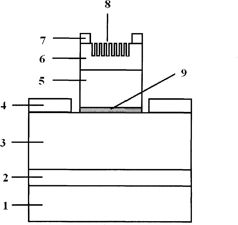
[0021] Firstly, the substrate 1 is cleaned, and the buffer layer 2 and the semiconductor epitaxial stacked structure are sequentially deposited on the substrate 1 by metal-organic chemical vapor deposition (MOCVD), molecular beam epitaxy (MBE) and other known semiconductor epitaxial growth methods. The epitaxial stack includes at least an N-type layer 3, a light-emitting layer 9 and a P-type GaN layer 5 from bottom to top; the light-emitting layer 9 usually has a quantum well structure.
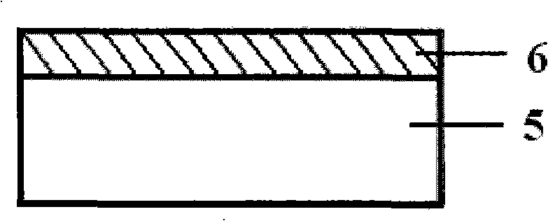
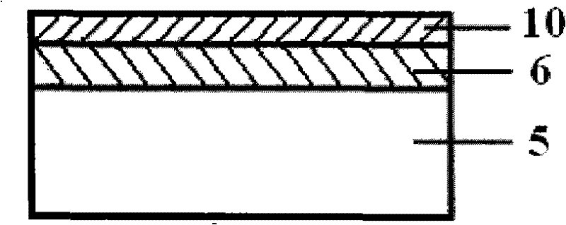
[0022] 2. Prepare a transparent conductive electrode 6 on the surface of the P-type GaN layer 5:
[0023] From the perspective of application, chemical vapor deposition (CVD) is the most promising method for the synthesis of CNT thin films. In this example,...
example 1
[0036] The substrate 1 is formed of Si, sapphire or GaN-based substrate material, and the semiconductor epitaxial stack is formed of Group III nitride material. In order to solve the problem of cracks in the semiconductor epitaxial stack or lattice mismatch with the substrate, a buffer layer 2 is also provided between the semiconductor epitaxial stack and the substrate 1 . At the same time, in order to ensure that the current injection can spread evenly to the surface of the P-type GaN layer 5 , a transparent conductive electrode 6 is also provided between the P-type GaN layer 5 and the P-type electrode 7 . The two-dimensional CNT thin film photonic crystal 8 prepared on the transparent conductive electrode 6 can effectively improve the light extraction efficiency of the semiconductor light emitting device.
example 2
[0038] Synthesize CNT raw material, and prepare transparent conductive electrode 6 on the surface of p-type GaN layer 5:
[0039] From the perspective of application, chemical vapor deposition (CVD) is the most promising method for the synthesis of CNT thin films. In this example, the CVD technology using alcohol as a carbon source is first used to prepare SiO on a large-area Si sheet by electron beam evaporation. 2 / Co thin film, SiO 2 The thickness of the Co film is 20-1000nm, preferably 50-200nm, and the thickness of the Co film is less than 0.5-5nm, preferably 0.5-2nm. The CVD temperature is 550-800°C, the preferred condition is 650-750°C, the alcohol flow rate is preferably 50-200Sccm, and the reaction time is 1-60min. By controlling the thickness of the Co film to control the diameter of the single-layer CNT, the work function of the single CNT can be adjusted. The obtained product is purified to obtain CNTs with a purity of not less than 90%;
[0040] Select the CN...
PUM
| Property | Measurement | Unit |
|---|---|---|
| thickness | aaaaa | aaaaa |
| thickness | aaaaa | aaaaa |
| thickness | aaaaa | aaaaa |
Abstract
Description
Claims
Application Information


