Production method for GaN based LED

A light-emitting diode, N-type technology, applied in the direction of semiconductor devices, electrical components, circuits, etc., can solve the problems of ITO supply limited by raw materials, high forward voltage, etc., to achieve improved light extraction efficiency, high production efficiency, and simple manufacturing process Effect

Inactive Publication Date: 2009-07-22
HUAZHONG UNIV OF SCI & TECH
View PDF0 Cites 18 Cited by
  • Summary
  • Abstract
  • Description
  • Claims
  • Application Information

AI Technical Summary

Problems solved by technology

However, ITO film is an N-type semiconductor, and it is difficult to form a good ohmic contact with P-GaN, so the forward voltage of ITO / P-GaN-based LEDs is too high to meet the application requirements
At the same time, due to the low content of metal In in nature, the supply of ITO is limited by raw materials

Method used


Image

  • Production method for GaN based LED
  • Production method for GaN based LED
  • Production method for GaN based LED

Examples


preparation example Construction

[0019] The invention provides a method for preparing a GaN-based light-emitting diode using a CNT film as a transparent conductive electrode. The method includes the following steps:

[0020] 1. Growth of semiconductor epitaxial layer:

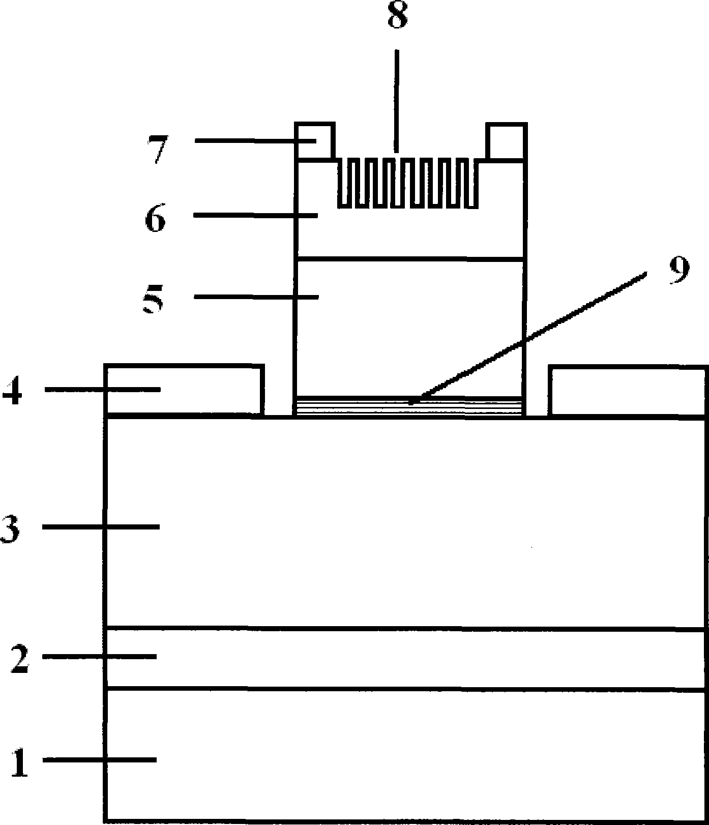
[0021] Firstly, the substrate 1 is cleaned, and the buffer layer 2 and the semiconductor epitaxial stacked structure are sequentially deposited on the substrate 1 by metal-organic chemical vapor deposition (MOCVD), molecular beam epitaxy (MBE) and other known semiconductor epitaxial growth methods. The epitaxial stack includes at least an N-type layer 3, a light-emitting layer 9 and a P-type GaN layer 5 from bottom to top; the light-emitting layer 9 usually has a quantum well structure.

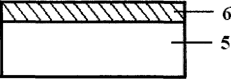
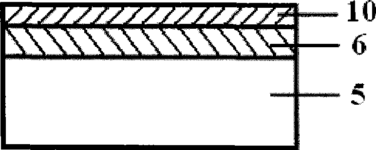
[0022] 2. Prepare a transparent conductive electrode 6 on the surface of the P-type GaN layer 5:

[0023] From the perspective of application, chemical vapor deposition (CVD) is the most promising method for the synthesis of CNT thin films. The wooden embod...

example 1

[0036] The substrate 1 is formed of Si, sapphire or GaN-based substrate material, and the semiconductor epitaxial stack is formed of Group III nitride material. In order to solve the problem of cracks in the semiconductor epitaxial stack or lattice mismatch with the substrate, a buffer layer 2 is also provided between the semiconductor epitaxial stack and the substrate 1 . At the same time, in order to ensure that the current injection can spread evenly to the surface of the P-type GaN layer 5 , a transparent conductive electrode 6 is also provided between the P-type GaN layer 5 and the P-type electrode 7 . The two-dimensional CNT thin film photonic crystal 8 prepared on the transparent conductive electrode 6 can effectively improve the light extraction efficiency of the semiconductor light emitting device.

example 2

[0038] Synthesize CNT raw material, and prepare transparent conductive electrode 6 on the surface of p-type GaN layer 5:

[0039] From the perspective of application, chemical vapor deposition (CVD) is the most promising method for the synthesis of CNT thin films. In this example, the CVD technology using alcohol as a carbon source is first used to prepare SiO on a large-area Si sheet by electron beam evaporation. 2 / Co thin film, SiO 2 The thickness of the Co film is 20-1000nm, preferably 50-200nm, and the thickness of the Co film is less than 0.5-5nm, preferably 0.5-2nm. The CVD temperature is 550-800°C, the preferred condition is 650-750°C, the alcohol flow rate is preferably 50-200Sccm, and the reaction time is 1-60min. By controlling the thickness of the Co film to control the diameter of the single-layer CNT, the work function of the single CNT can be adjusted. The obtained product is purified to obtain CNTs with a purity of not less than 90%;

[0040] Select the CN...


PUM

PropertyMeasurementUnit
thicknessaaaaaaaaaa
thicknessaaaaaaaaaa
thicknessaaaaaaaaaa

Abstract

The invention discloses a method for manufacturing GaN-based LED using a CNT thin film as a transparent conducting electrode, comprising growth of epitaxial layers of semiconductors, manufacturing of the transparent conducting electrode of the CNT thin film on the surface of a p-shaped GaN layer, manufacturing of two dimensional CNT thin film photonic crystal, formation of N-shaped metal electrode and manufacturing of P-shaped electrode. The method can effectively improve the light extracting rate of the front of LED and simultaneously solve the problem that the transparent conducting electrode contacts ohm of P-GaN. In terms of technique, materials of electrode are reasonably selected and nano-imprint technique is adopted, therefore, the method is characterized by low manufacturing cost and high production efficiency and grating resolution.

Description

technical field [0001] The invention relates to a light-emitting diode, in particular to a preparation method of a GaN-based light-emitting diode using a carbon nanotube (CNT) film as a transparent conductive electrode. Background technique [0002] The energy crisis has threatened the sustainable development of the economies of countries around the world, and the use of high-power GaN-based light-emitting diodes (LEDs) for lighting has become an important measure for countries to implement energy-saving strategies. Currently commercially available GaN-based LEDs basically use Ni / Au thin films as P electrodes. The reason for choosing metal Ni is that Ni is an ideal hydrogen adsorption material. After Au / Ni / P-GaN annealing, it can weaken the "hydrogen passivation" effect of P-GaN, thereby increasing the carrier concentration on the GaN surface, which is beneficial to Make a good ohmic contact. At the same time, in order to meet the requirements of front light emission, the ...

Claims


Application Information

Patent Timeline
Patent Type & Authority Applications(China)
IPC IPC(8): H01L33/00
Inventor 赵彦立元秀华黄黎蓉余永林刘文黄德修
Owner HUAZHONG UNIV OF SCI & TECH
Why Eureka
Try Eureka