Check patentability & draft patents in minutes with Patsnap Eureka AI!

Semiconductor device testing and sorting machine

A technology for testing sorting machines and semiconductors, which is applied in the direction of single semiconductor device testing, instrumentation, sorting, etc., and can solve the problems of low production efficiency, many equipment, and slow detection and sorting speed.

Inactive Publication Date: 2009-07-29
扬州市江都区东元机电设备有限公司
View PDF6 Cites 40 Cited by
  • Summary
  • Abstract
  • Description
  • Claims
  • Application Information

AI Technical Summary

Problems solved by technology

[0002] After the semiconductor device is manufactured, it needs to be inspected, marked, sorted, and taped and packaged. In the prior art, the above-mentioned work processes are carried out independently. low

Method used


Image

  • Semiconductor device testing and sorting machine
  • Semiconductor device testing and sorting machine

Examples


Embodiment Construction

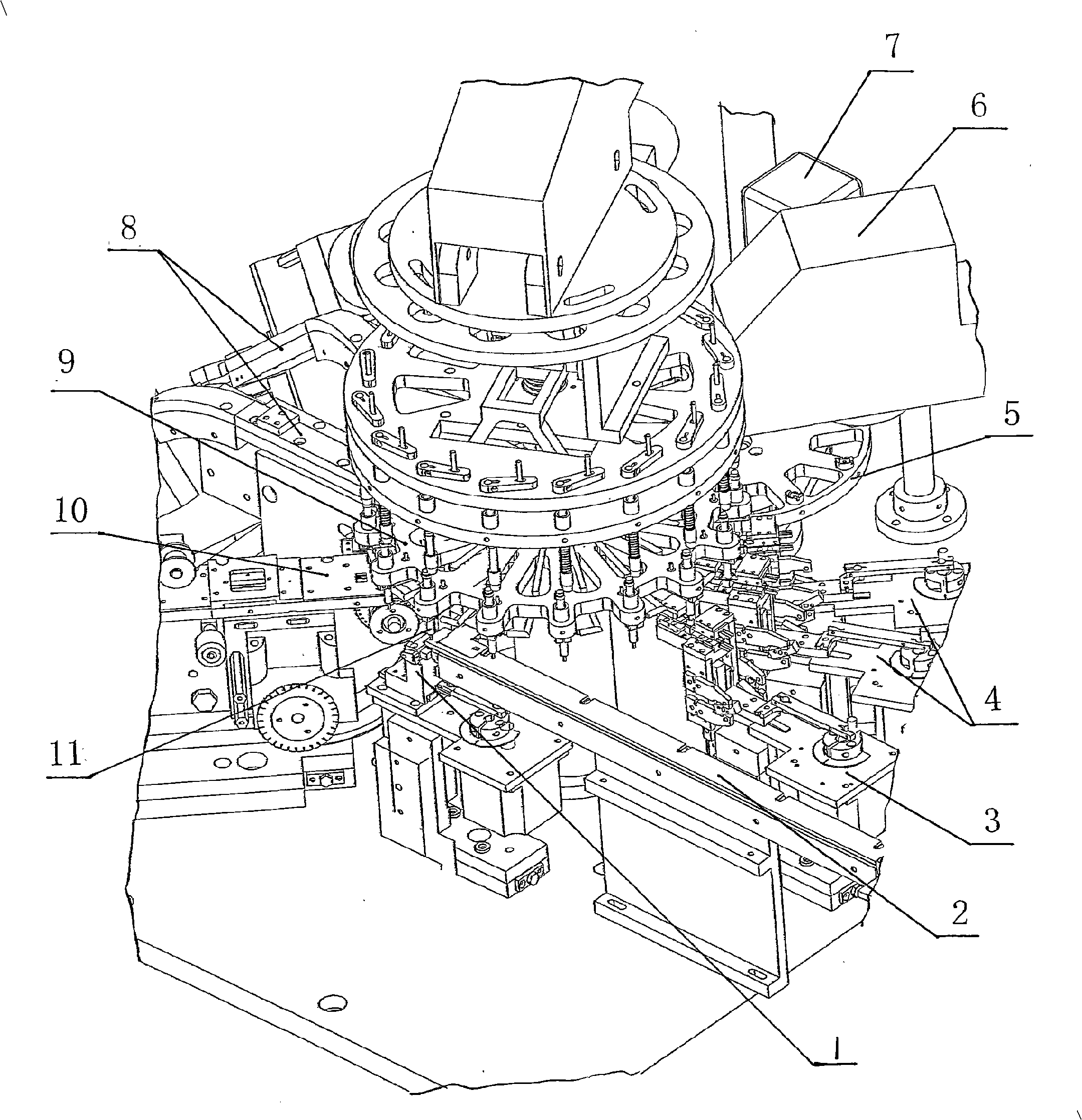
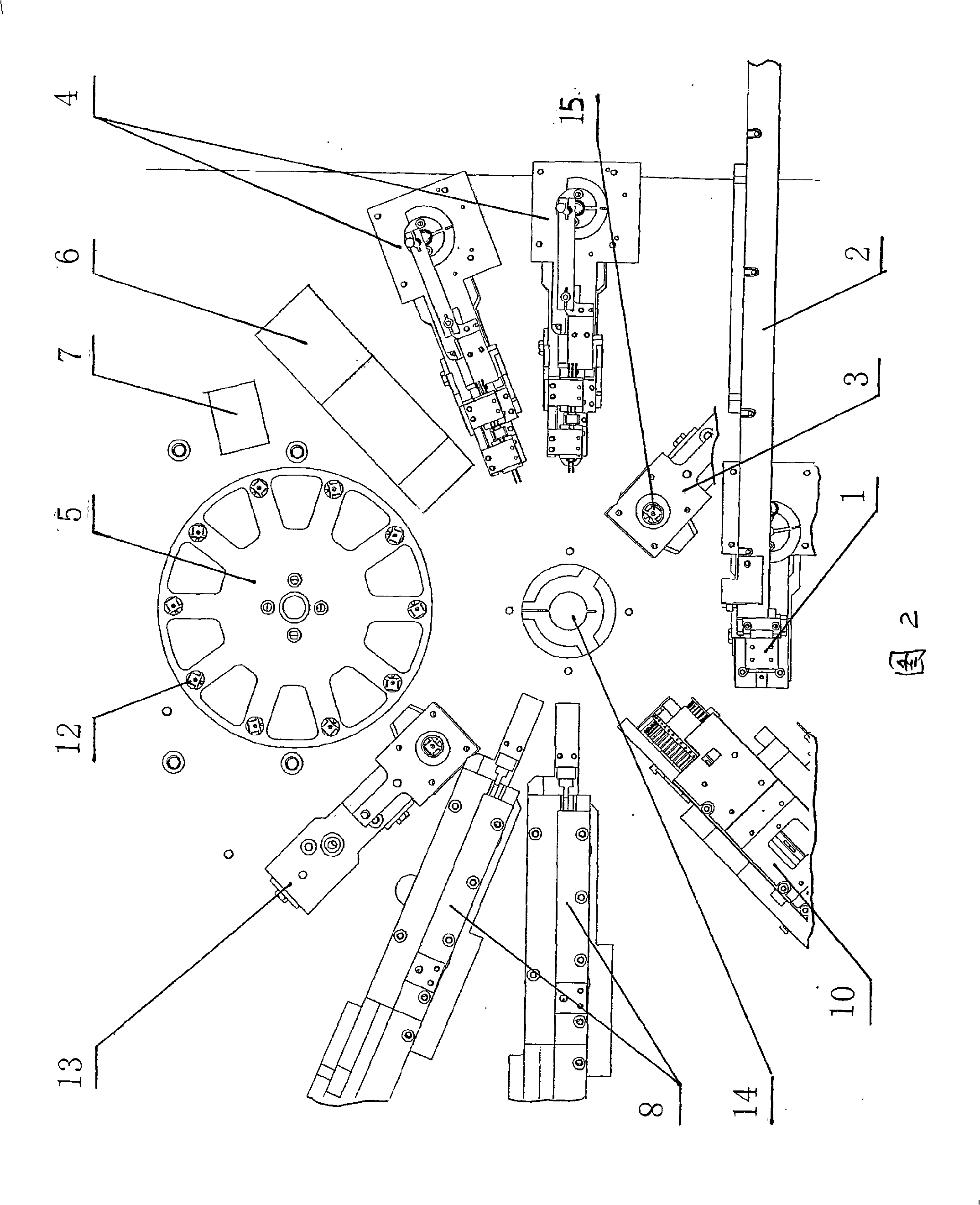
[0009] Such as figure 1 And 2, is a kind of semiconductor device test sorting machine, comprises the rotary table 9 that is arranged horizontally, and the rotary table 9 is installed on the upper end of the vertical shaft 14, and the outer circumference of the rotary table 9 is evenly distributed with a number of liftable suction nozzles 11, Around the rotary table 9, there are arranged in a clockwise direction a separation table 1 corresponding to the position of the suction nozzle 11, a first rotary positioning device 3, a detection head 4, an image camera 6, an auxiliary turntable 5, a second rotary positioning device 13, The unloading mechanism 8 and the braiding mechanism 10, the separation platform 1 is connected with the feeding mechanism 2, and the first rotary positioning device 3 and the second rotary positioning device 13 each include a mold cavity that is compatible with the detected device 15. The mold cavity 15 is just below the suction nozzle 11 of the correspon...


PUM


Abstract

The invention discloses a separator for testing semiconductor devices, belonging to the field of semiconductor device detection technique. The separator comprises a rotation workbench which is arranged at the upper end of a vertical shaft; the external circumference of the rotation workbench is uniformly provided with a plurality of liftable suction nozzles; the rotation workbench is sequentially provided with a separation platform, a first rotation positioning device, a detection head, an image camera, an auxiliary rotation disc, a second rotation positioning device, a blanking mechanism and a braiding mechanism which are arranged in clockwise direction or anticlockwise direction and corresponding to the positions of the suction nozzles; the separation platform is connected with the blanking mechanism; the first rotation positioning device and the second rotation positioning device respectively comprise a cavity which is adaptable for the device to be detected; the cavity is arranged below the suction nozzle at the corresponding working position; the circumference of the auxiliary rotation disc is uniformly provided with a plurality of concave cavities which can hold the device to be detected; and the side surface of the auxiliary rotation disc is provided with a marking laser head which is corresponding to the concave cavity. The separator leads a computer to control a plurality of detection devices to work cooperatively, can realize detection, marking, separating and braiding, and has compact structure and high efficiency.

Description

technical field [0001] The invention relates to a device for testing and sorting semiconductor devices. Background technique [0002] After the semiconductor device is manufactured, it needs to be inspected, marked, sorted, and taped and packaged. In the prior art, the above-mentioned work processes are carried out independently. low. Contents of the invention [0003] The object of the present invention is to provide a semiconductor device testing and sorting machine, so that the detection, marking, sorting and tape braiding of semiconductor devices can be realized on one machine. The device has a compact structure and high detection efficiency. [0004] The purpose of the present invention is achieved in the following way: a semiconductor device testing and sorting machine includes a horizontally arranged rotary table, the rotary table is installed on the upper end of the vertical shaft, and a number of liftable suction nozzles are evenly distributed on the outer circum...

Claims


Application Information

Patent Timeline
IPC IPC(8): G01R31/26G01B11/00G01R31/01B07C5/00
Inventor 贡瑞龙陆军梁天贵
Owner 扬州市江都区东元机电设备有限公司
Features
  • R&D
  • Intellectual Property
  • Life Sciences
  • Materials
  • Tech Scout
  • Unparalleled Data Quality
  • Higher Quality Content
  • 60% Fewer Hallucinations
Learn More