

A crystal device
A crystal and device technology, applied in the field of optical or laser crystal structure, can solve the problems of inability to coat, difficult to coat, reduce laser damage threshold and service life, etc., to expand the scope of use, avoid film damage, and increase damage threshold and the effect of laser power
- Summary
- Abstract
- Description
- Claims
- Application Information
AI Technical Summary
Problems solved by technology
Method used
Image

Examples
Embodiment Construction
[0027] The present invention will be further described in conjunction with the accompanying drawings and specific embodiments.
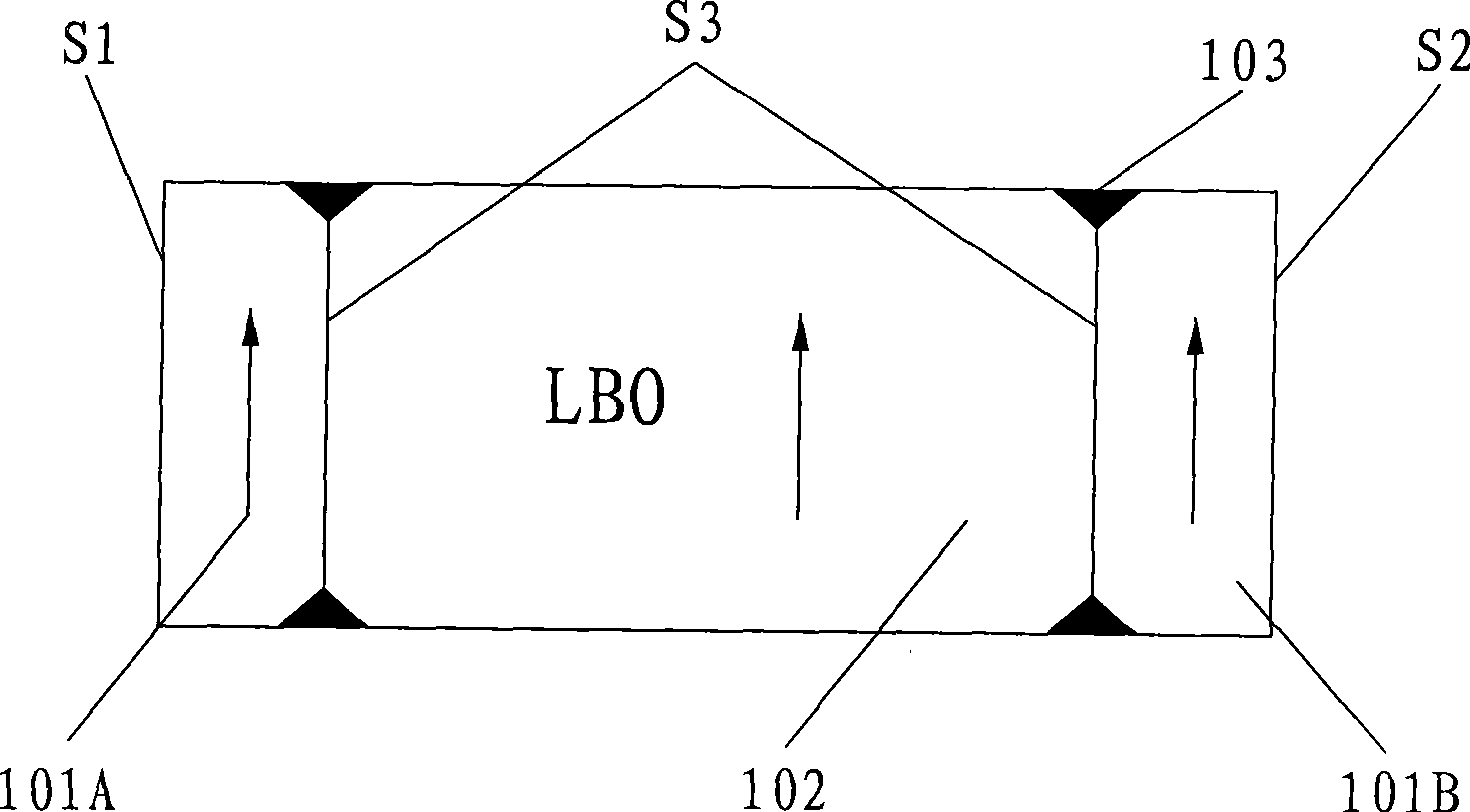
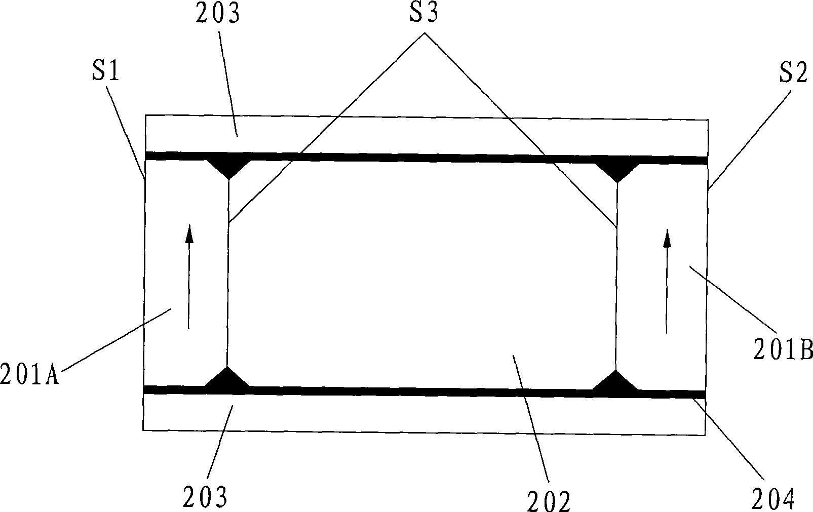
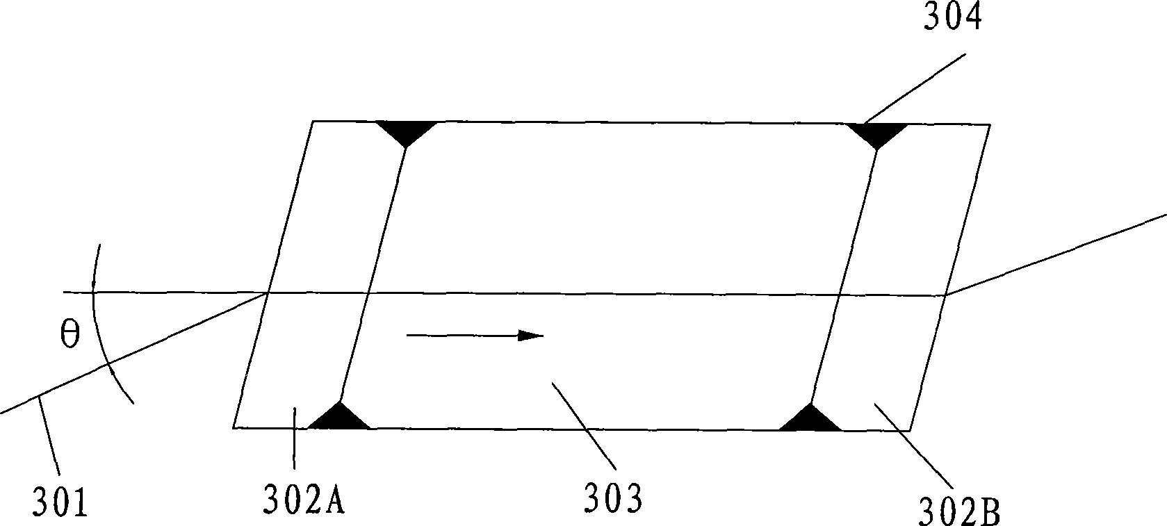
[0028] The crystal device of the present invention comprises a crystal, a first window, and a second window, wherein the first window is glued to the light-incident surface of the crystal, and the second window is glued to the light-emitting surface of the crystal. The crystal is a protected crystal, and no dielectric film is plated on the surface of the crystal. In order to improve light transmittance, a dielectric film can be coated on the first window plate or the second window plate, and an incident light anti-reflection film can be coated. The edges of the window and the nonlinear crystal are chamfered, and the glue is sealed with soft glue such as UV glue to make it difficult for moisture and dust to enter. Expanded, the opaque upper and lower bottom surfaces of the crystal may be provided with a protection sheet, and the protection sheet and ...
PUM
 Abstract
Description
Claims
Application Information