Semiconductor circuits capable of mitigating unwanted effects caused by input signal variations

A technology of semiconductors and circuits, applied in the field of semiconductor circuits that cause adverse effects due to changes, can solve the problems of consuming voltage margins and not being able to meet the needs of low voltages, etc.

Active Publication Date: 2009-08-12
MEDIATEK INC
View PDF0 Cites 4 Cited by
  • Summary
  • Abstract
  • Description
  • Claims
  • Application Information

AI Technical Summary

Problems solved by technology

[0003] However, the above solutions will consume the voltage head room, so the above solutions cannot meet the low voltage requirements of the new CMOS processing technology

Method used


Image

  • Semiconductor circuits capable of mitigating unwanted effects caused by input signal variations
  • Semiconductor circuits capable of mitigating unwanted effects caused by input signal variations
  • Semiconductor circuits capable of mitigating unwanted effects caused by input signal variations

Examples


Embodiment Construction

[0018] In order to make the purpose, features and advantages of the present invention more comprehensible, preferred embodiments are specifically cited below and described in detail with accompanying drawings. The description of the present invention provides different examples to illustrate the technical features of different implementations of the present invention. Wherein, the configuration of each element in the embodiment is used to illustrate the present invention, but not to limit the present invention. In addition, part of the reference numerals in the embodiments are repeated for the purpose of simplifying the description, and do not imply the correlation between different embodiments.

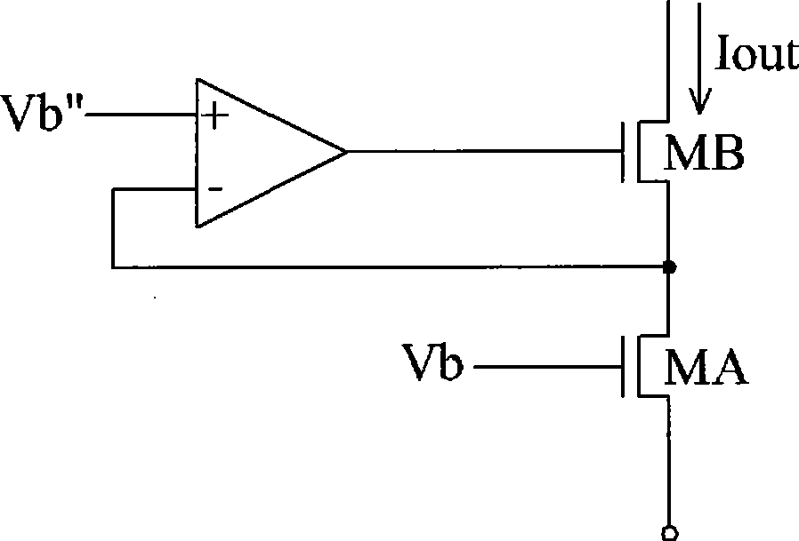
[0019] Figure 4 is a schematic circuit diagram showing a semiconductor circuit according to an embodiment of the present invention. The semiconductor circuit 100 includes a master circuit 10 and a replica circuit 20 . The main circuit 10 is a differential amplifier, which outputs...


PUM


Abstract

A stanchion system, includes a stanchion post and an attachment system for attachment to a flange which includes a first edge and a second edge. The attachment system includes a crossbar including an extending section and an abutment member on a first end thereof to abut the first edge of the flange; a base including a passage through which the extending section of the crossbar is movable and a seating for the stanchion post; and a connector including a first section and a second section. The second section of the connector is attachable to the extending section of the crossbar at one of a plurality of incremental positions. The first section of the connector is movable relative to the second section to adjust the position of the first section relative to the abutment member of the crossbar. In several embodiments, the first section is movable relative to the second section to abut the base on a side of the base opposite the side upon which the flange is positioned to adjust the position of the first section relative to the abutment member.

Description

technical field [0001] The present invention relates to a semiconductor circuit, and more particularly to a semiconductor circuit capable of alleviating adverse effects caused by fluctuations in received input signals. Background technique [0002] In most analog circuits, the current source is one of the most basic components that determine the performance of the overall circuit. Therefore, in analog circuits, a current source with a large output impedance is usually required. In a complementary metal-oxide-semiconductor circuit (CMOS), a simple current source such as figure 1 shown. The source and the gate of the NMOS transistor MA are respectively connected to a constant voltage, and the drain is an output node of the current source. Such a simple circuit cannot provide a large enough output impedance, and further, if figure 2 As shown, another NMOS transistor MB is cascaded to the current source (ie: MA), and the output impedance is increased by clamping the voltage ...

Claims


Application Information

Patent Timeline
Patent Type & Authority Applications(China)
IPC IPC(8): G05F1/46G05F1/56H03F3/14
Inventor 胡思全洪志谦
Owner MEDIATEK INC
Why Eureka
Try Eureka