Method for manufacturing hyperconjugation VDMOS device

A device and lithography technology, which is applied in the field of preparation of power metal oxide semiconductor field effect transistor devices to achieve the effects of reducing on-resistance and on-state power consumption

Active Publication Date: 2011-02-16
BEIJING ZHONGKE XINWEITE SCI & TECH DEV
View PDF0 Cites 2 Cited by
  • Summary
  • Abstract
  • Description
  • Claims
  • Application Information

AI Technical Summary

Problems solved by technology

[0005] The on-resistance of traditional VDMOS power devices is limited by the breakdown voltage and there is a limit - called "silicon limit", which cannot be lowered any further

Method used


Image

  • Method for manufacturing hyperconjugation VDMOS device
  • Method for manufacturing hyperconjugation VDMOS device
  • Method for manufacturing hyperconjugation VDMOS device

Examples


Embodiment Construction

[0039] In order to make the object, technical solution and advantages of the present invention clearer, the present invention will be described in further detail below in conjunction with specific embodiments and with reference to the accompanying drawings.

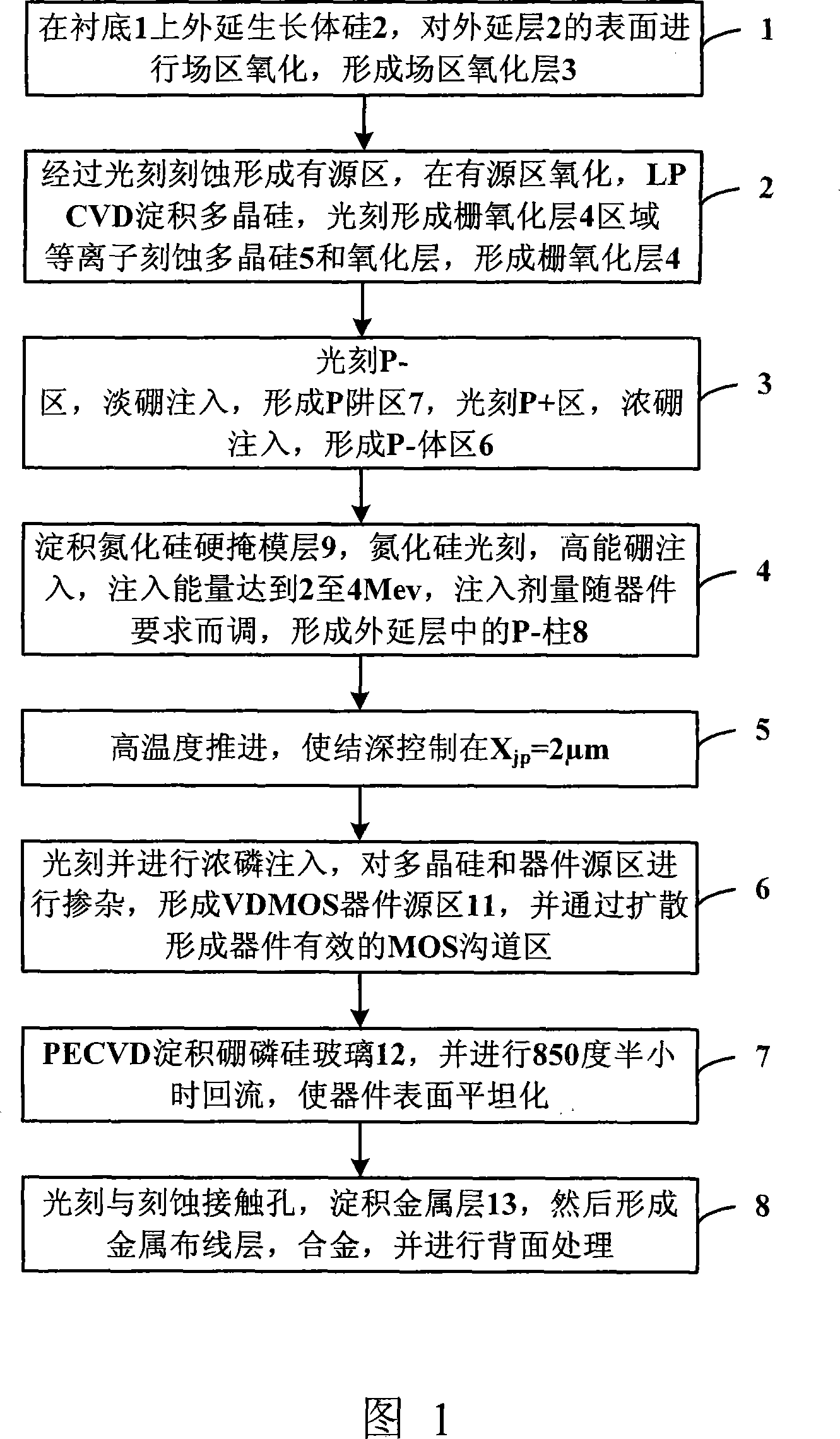
[0040] like figure 1 as shown, figure 1 It is a flow chart of a method for preparing a super junction VDMOS provided by the present invention, and the method includes the following steps:

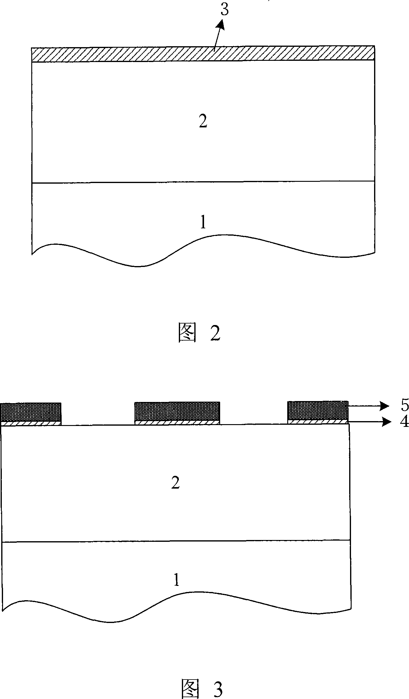
[0041] Step 1, epitaxially growing bulk silicon 2 on the substrate 1, performing field oxidation on the surface of the epitaxial layer 2, to form a field oxide layer 3;

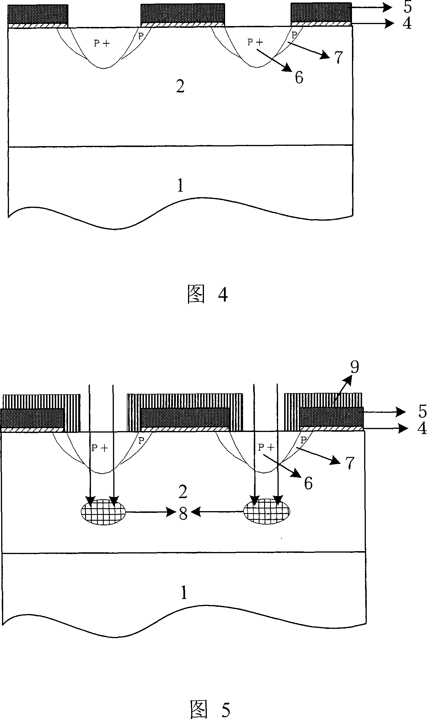
[0042] Step 2, forming an active area through photolithography, oxidation in the active area, LPCVD deposition of polysilicon, photolithography to form the area of ​​the gate oxide layer 4, plasma etching of the polysilicon 5 and the oxide layer to form the gate oxide layer 4;

[0043] Step 3, photoetching the P-region, implanting light boron to form the P well re...


PUM


Abstract

The invention discloses a method for manufacturing a hyperconjugation VDMOS device, which comprises the following steps: growing body silicon on a substrate by epitaxy, oxidizing a zone to form a zone oxidizing layer; etching the zone to form an active area, oxidizing the active area, depositing polycrystalline silicon on LPCVD, photoetching the active area to form a gate oxidizing layer, and etching the polycrystalline silicon and the oxidizing layers to form a gate oxidizing layer by plasma; photoetching a P-area, injecting dilute boron into the P-area to form a P well area, photoetching a P+area, and injecting concentrated boron into the P+area to form a P-body area; depositing a silicon nitride hard mask layer, photoetching silicon nitride, injecting high-energy boron into the siliconnitride hard mask layer to form a P-column in an epitaxial layer; boosting the P-column at high temperature, and controlling the junction depth Xjp to be 2mu m; photoetching the P-column and injecting concentrated phosphorus into the P-column, doping the polycrystalline silicon and a device source area to form a VDMOS device source area, and diffusing the VDMOS device source area to form an efficient MOS device channel area; depositing boron-phosphorus-silicon glass on PECVD, and reflowing the boron-phosphorus-silicon glass for half an hour at a temperature of 850 DEG C; and photoetching and etching contact holes, depositing a metal layer to form a metal wiring layer, alloying the layer, and carrying out back treatment.

Description

technical field [0001] The invention relates to the technical field of semiconductor devices and manufacturing techniques thereof, in particular to a preparation method of power metal oxide semiconductor field effect transistor (VDMOS) devices. Background technique [0002] Power metal oxide semiconductor field effect transistor is a new type of power device developed rapidly in recent years, because it has many excellent properties than bipolar power devices: such as high input impedance, low drive current, no minority carrier storage effect, fast switching speed , high operating frequency, negative current temperature coefficient, and good current self-regulation ability, which can effectively prevent local current concentration and hot spots, even current distribution, easy to increase current capacity through parallel connection, and strong power Processing capacity, good thermal stability, large safe working area, no secondary breakdown, etc., have been widely used in v...

Claims


Application Information

Patent Timeline
Patent Type & Authority Patents(China)
IPC IPC(8): H01L21/336
Inventor 蔡小五海潮和陆江王立新
Owner BEIJING ZHONGKE XINWEITE SCI & TECH DEV
Why Eureka
Try Eureka