Supercharge Your Innovation With Domain-Expert AI Agents!

Method for manufacturing single-electron memory

A memory and single-electron technology, which is applied in semiconductor/solid-state device manufacturing, circuits, electrical components, etc., can solve the problems of relying on electron beam lithography for secondary alignment and complex process steps, and achieve low power consumption and few process steps , the effect of large consistency

Active Publication Date: 2011-01-26
成都豆萁集成电路设计有限公司
View PDF0 Cites 0 Cited by
  • Summary
  • Abstract
  • Description
  • Claims
  • Application Information

AI Technical Summary

Problems solved by technology

[0004] In order to solve the shortcomings of the existing single-electron memory preparation technology, such as complicated process steps and over-reliance on the secondary alignment of electron beam lithography, the purpose of the present invention is to provide a preparation method of a single-electron memory, which has a simple preparation process and can Compatible with conventional microelectronics processes

Method used


Image

  • Method for manufacturing single-electron memory
  • Method for manufacturing single-electron memory
  • Method for manufacturing single-electron memory

Examples


Embodiment Construction

[0029] The technical solution of the present invention will be described in detail below in conjunction with the drawings and embodiments.

[0030] The present invention is a method for preparing a single-electron memory, and the specific process steps are as follows:

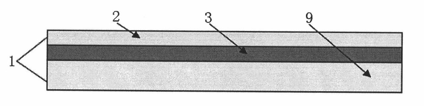
[0031] (1) Using p-type, The crystal-oriented 2-inch SOI is used as the substrate. The top silicon 2 of the substrate is 50nm thick, the buried oxide layer 3 is 375nm thick, the bulk silicon layer is 5000±100nm thick, and the resistivity of the top silicon 2 is figure 1 Shown

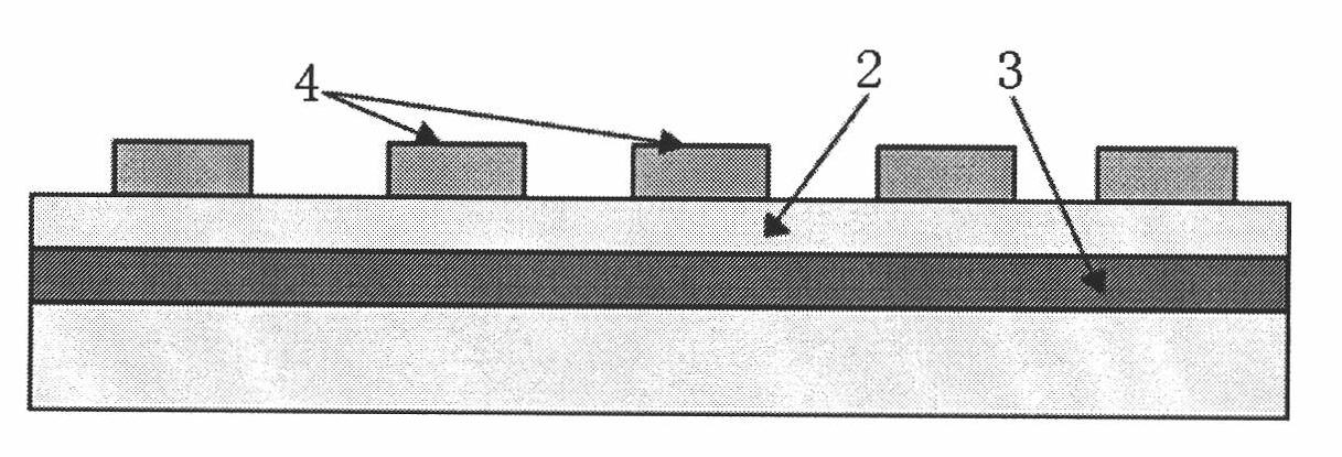
[0032] (2) Spin-coating Zep520 photoresist on SOI substrate 1, after exposure by electron beam lithography, developing, fixing, and drying with high-purity nitrogen to obtain the glue pattern of source, drain electrode, conductive channel, glue pattern 4 The shape on the SOI substrate 1 is like figure 2 Shown

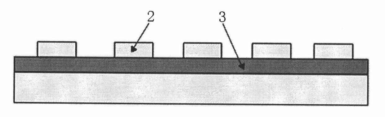
[0033] (3) Use wet etching to transfer the glue pattern 4 to the top layer silicon 2. The wet etching solution uses HNO 3 , H 2 O and...


PUM


Abstract

The invention provides a method for manufacturing a single-electron memory, which relates to the technical field of nano-devices. In order to overcome the defect of complicated technical steps in the The invention provides a method for manufacturing a single-electron memory, which relates to the technical field of nano-devices. In order to overcome the defect of complicated technical steps in themd by the method has great consistency, low operating voltage and low power consumption.tured by the method has great consistency, low operating voltage and low power consumption.anufacturing technology of the prior single-electron memory, the invention aims at providing the method for manufacturing the single-electron memory. An electrode pattern and a conductive channel aremanufacturing technology of the prior single-electron memory, the invention aims at providing the method for manufacturing the single-electron memory. An electrode pattern and a conductive channel are manufactured by adopting electron beam photoetching technology and photoetching technology, source and drain contact electrodes are manufactured by an optical photoetching and stripping method, thin-manufactured by adopting electron beam photoetching technology and photoetching technology, source and drain contact electrodes are manufactured by an optical photoetching and stripping method, thin-layer silicon is manufactured by an electron beam evaporating method, then, the thin-layer silicon on the surface is manufactured into silicon quantum dots by flash annealing technology, and finally,layer silicon is manufactured by an electron beam evaporating method, then, the thin-layer silicon on the surface is manufactured into silicon quantum dots by flash annealing technology, and finally,gate electrodes are manufactured by stripping technology. The invention has simple technical steps and is compatible with the traditional microelectronic technology. The single-electron memory manufacgate electrodes are manufactured by stripping technology. The invention has simple technical steps and is compatible with the traditional microelectronic technology. The single-electron memory manufacture

Description

Technical field [0001] The invention relates to the technical field of nano device manufacturing, in particular to a method for preparing a single electron memory. Background technique [0002] For more than half a century, semiconductor integrated circuits with CMOS as the mainstream technology have been developing rapidly in accordance with "Moore's Law", and their feature sizes have entered the nanometer level, but they are also facing more and more serious challenges. Therefore, they are based on new materials. , Nanoelectronic devices with new principles, such as various quantum dot devices, nanowires, nanotube devices, single-electron devices, single-electron memory, etc. have become research hotspots. With the continuous reduction of global consumable resources, the production of various devices with low energy consumption has become a focus of research, including single-electron devices and single-electron memory components based on the Coulomb blockade effect. [0003] Th...

Claims


Application Information

Patent Timeline
Patent Type & Authority Patents(China)
IPC IPC(8): H01L21/8239
Inventor 贾锐李维龙陈晨朱晨昕李昊峰张培文刘明
Owner 成都豆萁集成电路设计有限公司
Features
  • R&D
  • Intellectual Property
  • Life Sciences
  • Materials
  • Tech Scout
  • Unparalleled Data Quality
  • Higher Quality Content
  • 60% Fewer Hallucinations
Learn More