

Pin bonding structure
A bonding structure and pin technology, which is applied in the directions of optics, instruments, electrical components, etc., can solve problems affecting the yield rate, misalignment at both ends of the X direction, and reduction of overlapping area, so as to improve the yield rate, ensure circuit connection performance, The effect of a large overlapping area
- Summary
- Abstract
- Description
- Claims
- Application Information
AI Technical Summary
Problems solved by technology
Method used
Image

Examples
Embodiment 1
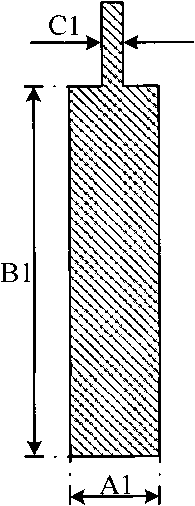
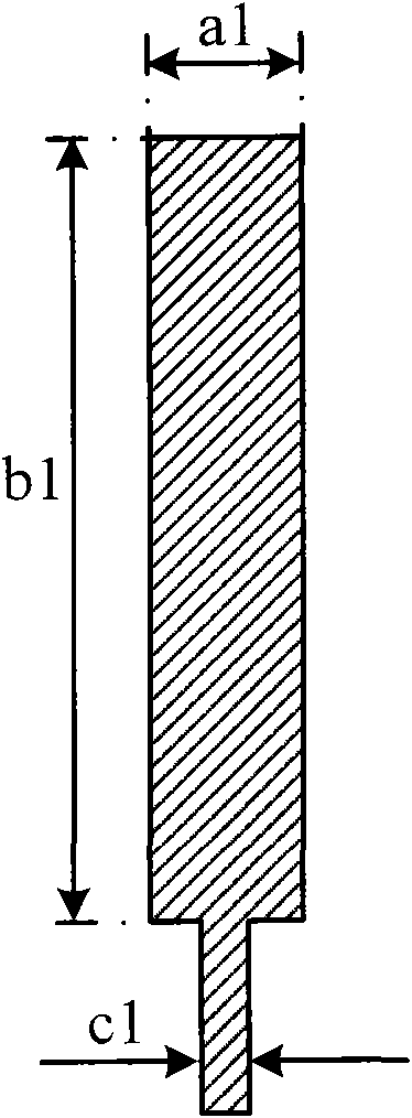
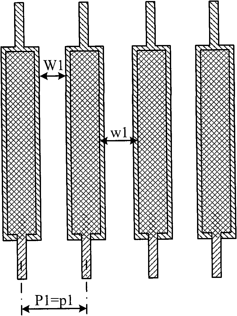
[0021] This embodiment provides a pin bonding structure such as image 3 shown, including panel pins and driver IC pins. Wherein, the panel pin includes a first pad portion 11 and a first lead portion 12 ; the driver IC pin includes a second pad portion 21 and a second lead portion 22 . Wherein, the part shown in the right slash shade represents the panel pin, the left slash shading part represents the drive IC pin, and the grid line shading represents the overlapping part of the panel pin and the drive IC pin.
[0022] The first pad portion 11 of the panel pin matches the size and shape of the second pad portion 21 of the drive IC pin; the first pad portion 11 and the second pad portion 21 corresponding to the position bonded together to form pad pairs. The pads are divided into upper and lower rows, and the lower edge of the upper row of pad pairs is higher than the upper edge of the lower row of pad pairs. Specifically, one of the two adjacent pad pairs is located in the...
Embodiment 2
[0030] On the basis of Embodiment 1, this embodiment provides various lead bonding structures by changing the relative positional relationship between the lead part and the pad part.
[0031] in such as Figure 5A In the structure shown, one of the two adjacent pad pairs is located in the upper left row, and the other is located in the lower right row. Among them, in the center of the pads in the upper left row, the first lead part 121 of the panel pin is located on the left side of the first pad part 111; the second lead part 221 of the drive IC pin is located in the second pad part 211 on the left side. Located in the pad pair in the lower right row, the first lead part 122 of the panel pin is located on the right side of the first pad part 112; the second lead part 222 of the drive IC pin is located at the side of the second pad part 212 middle part.
[0032] in such as Figure 5B In the structure shown, one of the two adjacent pad pairs is located in the lower left row...
PUM
| Property | Measurement | Unit |
|---|---|---|
| elongation | aaaaa | aaaaa |
Abstract
Description
Claims
Application Information