Semiconductor device and method for manufacturing the same
A manufacturing method, semiconductor technology, applied in the direction of semiconductor/solid-state device manufacturing, semiconductor devices, transistors, etc.
- Summary
- Abstract
- Description
- Claims
- Application Information
AI Technical Summary
Problems solved by technology
Method used
Image

Examples
no. 1 approach
Hereinafter, the structure of the semiconductor device according to the first embodiment of the present invention will be described with reference to the drawings.
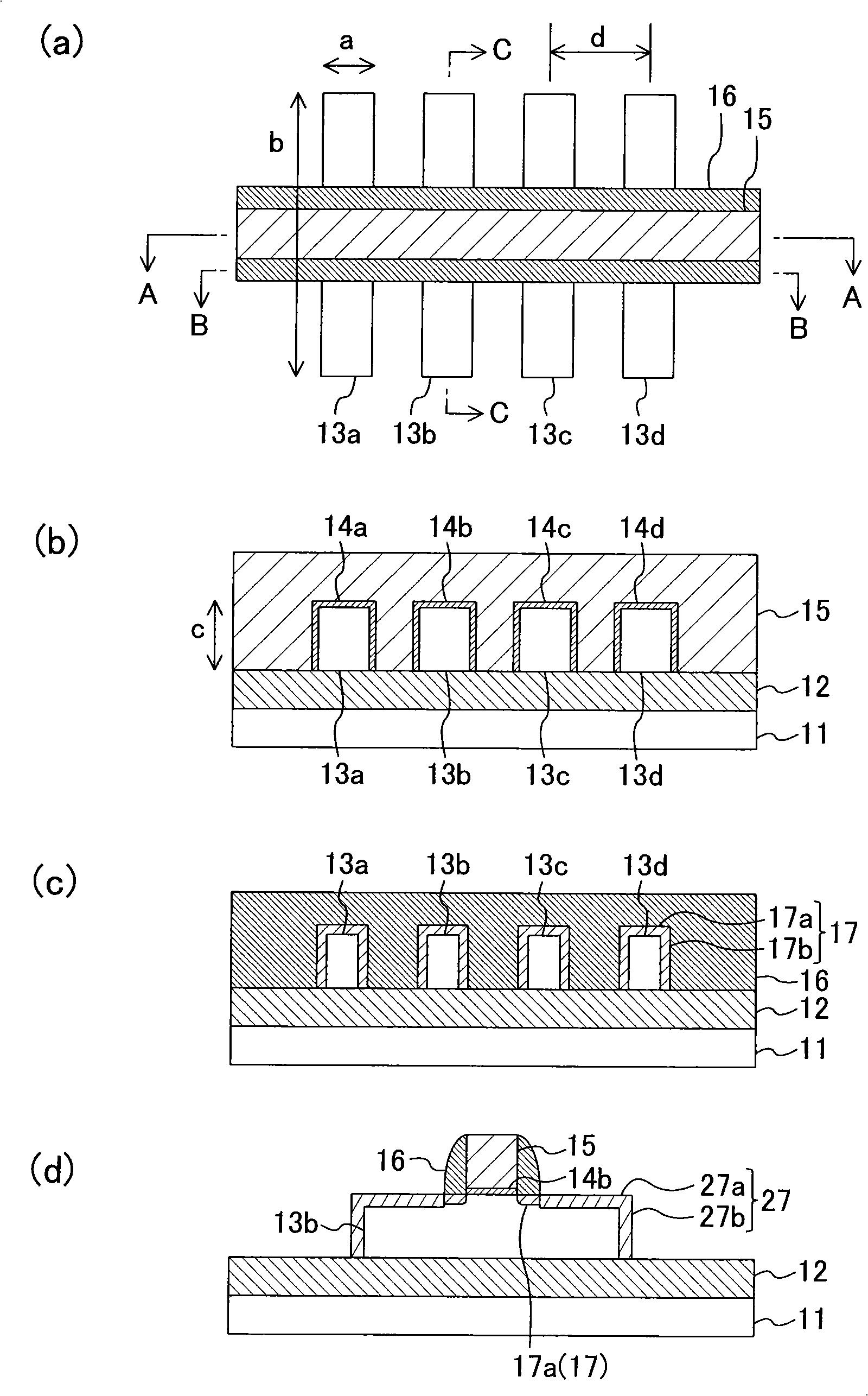
[0062] figure 1 (a) to (d) are structural diagrams showing a semiconductor device according to the first embodiment of the present invention, specifically, a semiconductor device having a fin field effect transistor, figure 1 (a) is a plan view, figure 1 (b) for figure 1 (a) A-A line sectional view, figure 1 (c) for figure 1 (a) B-B line sectional view, figure 1 (d) for figure 1 (a) C-C line sectional view.
[0063] The Fin Field Effect Transistor of this embodiment, such as figure 1 As shown in (a) to (d), there is a support substrate 11 made of, for example, silicon, an insulating layer 12 formed on the support substrate 11, for example, made of silicon oxide, and a fin-shaped semiconductor region formed on the insulating layer 12. 13a to 13d, the gate electrode 15 formed on the fin-shaped semico...
no. 1 example
In the first embodiment, by performing plasma doping at a pressure of 0.6 Pa or less, the amount of chipping at the upper corner (fin corner) of the fin-shaped semiconductor region can be suppressed, and the Highly uniform doping characteristics.
[0087] [Suppression of the amount of chipping at the corner of the fin]
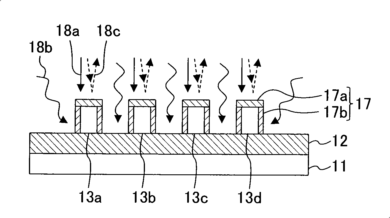
First, refer to Figure 4 (a) and (b) explain about suppression of the chipping amount of the fin corner part in the first embodiment.
[0088] Figure 4 (a) schematically shows the cross-sectional shape of the fin-shaped semiconductor region (more precisely, the fin-shaped semiconductor region 51 ) before plasma doping is performed. Here, the height and width of the fins are 120nm and 160nm, and the distance between the fins is 210nm. In other words, the distance between the widthwise center of the fin and the fin widthwise center of the partition wall was 370 nm. Also, the radius of curvature of the fin corners (in the dotted line area in the figure) is 8...
no. 2 example
In the second embodiment, by setting the pressure at the time of plasma doping to 0.6 Pa or more and 10 Pa or less and making the ionization current density Ii (mA / cm 2 ) and the pressure P (Pa) during plasma doping, the relationship is Ii≤0.52Ln(P)+0.36. Plasma doping can achieve high uniform doping while suppressing the amount of chipping at the corner of the fin. Miscellaneous. Also, Ln represents a natural logarithm.
[0105] In the second embodiment, as the fin-shaped semiconductor region (before plasma doping) for checking the chipping amount of the fin-shaped corner portion, the same Figure 4 (a) The same sample as shown in the first embodiment. In other words, the height and width of the fins are 120nm and 160nm, and the distance between the fins is 210nm. In other words, the distance between the center of the fin in the width direction and the center of the fin in the partition wall in the width direction was 370 nm. Also, the radius of curvature of the fin-shaped...
PUM
 Abstract
Description
Claims
Application Information
 - R&D Engineer
- R&D Manager
- IP Professional
- Industry Leading Data Capabilities
- Powerful AI technology
- Patent DNA Extraction
Browse by: Latest US Patents, China's latest patents, Technical Efficacy Thesaurus, Application Domain, Technology Topic.
© 2024 PatSnap. All rights reserved.Legal|Privacy policy|Modern Slavery Act Transparency Statement|Sitemap