Array substrate, manufacturing method thereof and display device
A technology of an array substrate and a manufacturing method, applied in the display field, can solve problems such as poor fog, affecting product quality, Ioff, etc., and achieve the effects of avoiding pollution, avoiding deterioration of TFT characteristics, and improving product quality
- Summary
- Abstract
- Description
- Claims
- Application Information
AI Technical Summary
Problems solved by technology
Method used
Image

Examples
Embodiment Construction
[0051] The specific implementation manners of the present invention will be further described in detail below in conjunction with the accompanying drawings and embodiments. The following examples are used to illustrate the present invention, but are not intended to limit the scope of the present invention.
[0052] Such as Figure 2a ~ 2g As shown, the method for fabricating an array substrate in this embodiment includes the following steps:
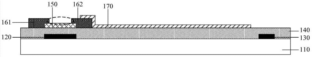
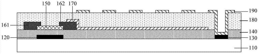
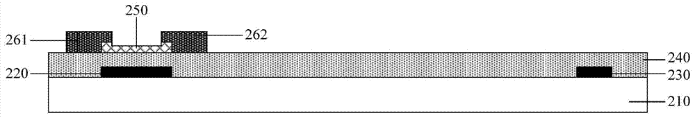
[0053] Step one, such as Figure 2aAs shown, a pattern including a gate line (not shown in the figure), a gate 220, a common electrode line 230 and a gate insulating layer 240 is formed on the base substrate 210 (the gate 220, the gate line and the common electrode line 230 are formed at the same time Formed in the patterning process, only one mask is needed). The gate insulating layer 240 is formed on the gate line, the gate electrode 220 and the common electrode 230 . The specific process flow and the formed graphic structure of th...
PUM
 Abstract
Description
Claims
Application Information