Semiconductor module manufacturing method and semiconductor module
a semiconductor module and manufacturing method technology, applied in the direction of semiconductor devices, semiconductor/solid-state device details, electrical apparatus, etc., can solve the problems of deterioration of semiconductor module characteristics, increased electrical continuity of pin-shaped external terminals,
- Summary
- Abstract
- Description
- Claims
- Application Information
AI Technical Summary
Benefits of technology
Problems solved by technology
Method used
Image

Examples
first embodiment
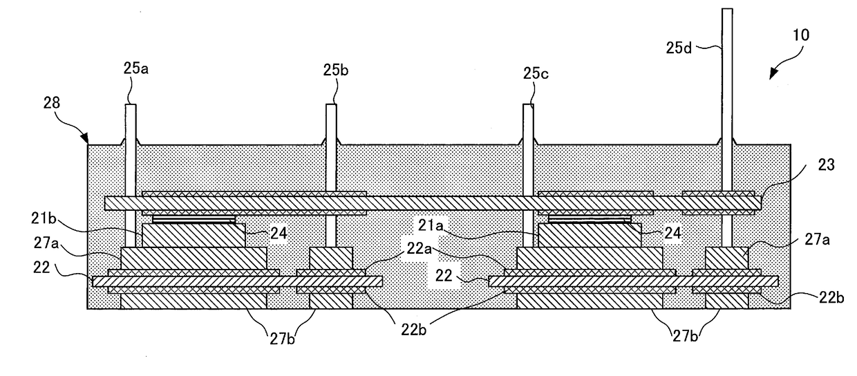
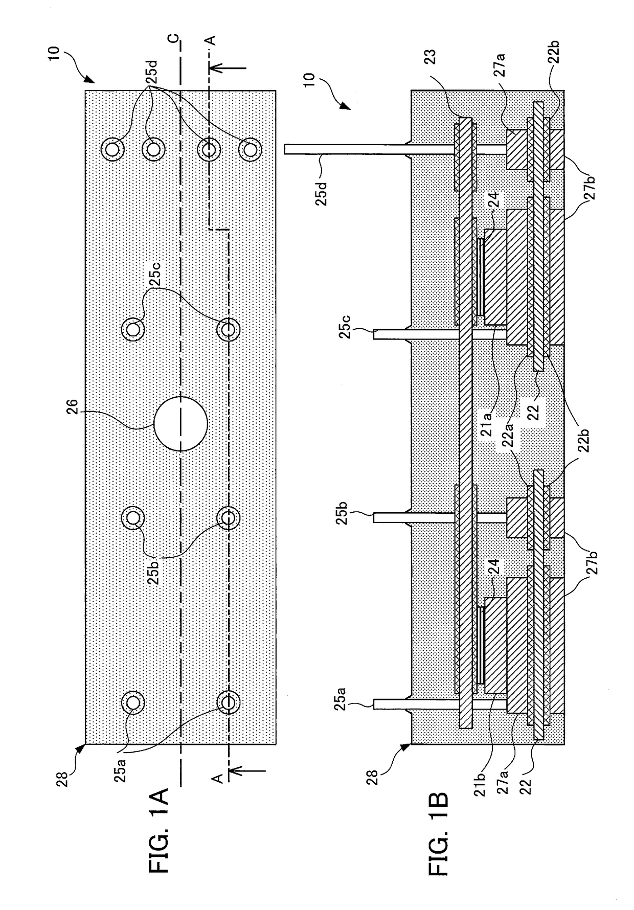
[0032]A semiconductor module 10 according to a first embodiment will be described with reference to FIGS. 1A and 1B and FIG. 2.
[0033]FIGS. 1A and 1B illustrate the semiconductor module 10 according to the first embodiment.
[0034]FIG. 1A is a top view of the semiconductor module 10, and FIG. 1B is a sectional view of the semiconductor module 10, taken along an alternate long and short dash line A-A in FIG. 1A.
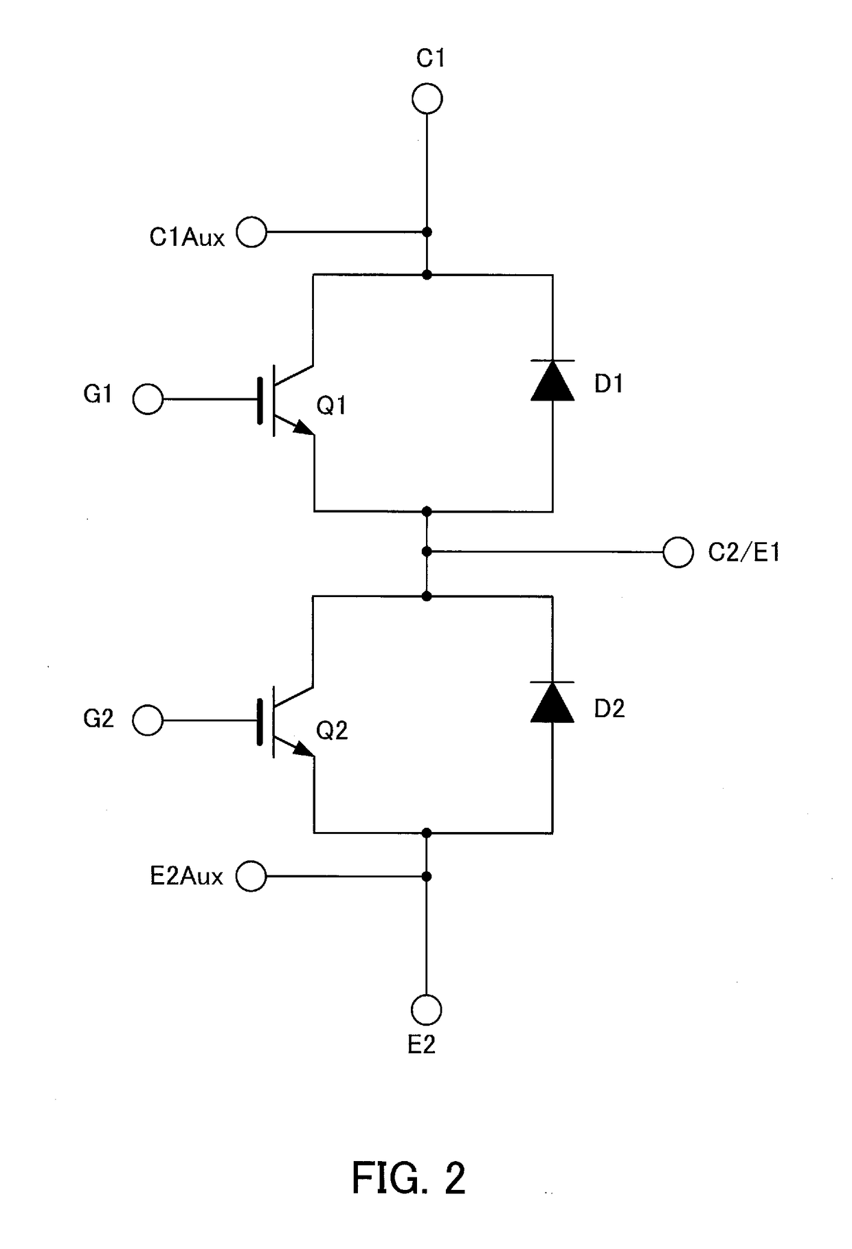
[0035]FIG. 2 is an equivalent circuit illustrating a circuit configuration of the semiconductor module 10 according to the first embodiment.
[0036]The semiconductor module 10 includes two sets of semiconductor circuits and a wiring substrate 23 forming a common wiring circuit above the semiconductor circuits. One of the two sets of semiconductor circuits is configured by mounting a semiconductor chip 21a on an insulating substrate 22, and the other set of semiconductor circuits is configured by mounting a semiconductor chip 21b on another insulating substrate 22. The semiconductor...
second embodiment
[0084]Next, a second embodiment will be described with reference to FIG. 11. In the second embodiment, an individual external terminal 25 is provided with an outflow prevention portion different from that according to the first embodiment.
[0085]FIG. 11 illustrates a pin-shaped external terminal of a semiconductor module according to the second embodiment.
[0086]In the second embodiment, as illustrated in FIG. 11, the outer surface portion of the external terminal 25 is provided with an outflow prevention portion 40 made of an elastic member having excellent heat resistance such as a silicone rubber.
[0087]By forming this outflow prevention portion 40 on the external terminal 25, the same advantageous effects as those in the first embodiment are also obtained. Namely, when the external terminal 25 is placed in the transfer molding die 100, the outflow prevention portion 40 of the external terminal 25 is sandwiched between the fixed lower die 110 and the movable lower die 120 combined w...
third embodiment
[0089]Next, a third embodiment will be described with reference to FIG. 12. In the third embodiment, an individual external terminal 25 is provided with at least one outflow prevention portion different from those according to the first and second embodiments.
[0090]FIG. 12 illustrates a pin-shaped external terminal 25 of a semiconductor module according to a third embodiment.
[0091]The upper part of FIG. 12 illustrates a top view of the external terminal 25, and the lower part of FIG. 12 illustrates a side view of the external terminal 25.
[0092]In the third embodiment, as illustrated in FIG. 12, two pairs of depressed portions 25g1 and 25g2 are formed vertically in a longitudinal direction of the external terminal 25. More specifically, the two pairs are formed on two sides of the outer surface portion of the external terminal 25, respectively. By forming a pair of depressed portions 25g1 and 25g2, a protruded portion is formed therebetween as an outflow prevention portion 25f.
[0093...
PUM
 Abstract
Description
Claims
Application Information
 - R&D Engineer
- R&D Manager
- IP Professional
- Industry Leading Data Capabilities
- Powerful AI technology
- Patent DNA Extraction
Browse by: Latest US Patents, China's latest patents, Technical Efficacy Thesaurus, Application Domain, Technology Topic.
© 2024 PatSnap. All rights reserved.Legal|Privacy policy|Modern Slavery Act Transparency Statement|Sitemap