This helps you quickly interpret patents by identifying the three key elements:
Problems solved by technology
Method used
Benefits of technology
Problems solved by technology
In addition, since the solder material is pasty, there is a problem that flux components or solder material scatter during reflow.
[0011] In addition, with the recent miniaturization of semiconductor elements, the weight of the semiconductor element 105 itself has become lighter. If a paste-like solder material is applied by printing, the semiconductor element 105 will move, and the application position of the paste-like solder will occur. problems such as deviation
[0012] Furthermore, there are variations in the heights of the post electrodes 112a, and in post electrodes with a relatively short distance, there is a problem that the lower part of the post electrodes and the electrodes cannot be sufficiently bonded through the solder layer.
Method used
Image
Click on the blue label to locate the original text in one second.
Reading with bidirectional positioning of images and text.
Examples
no. 1 approach
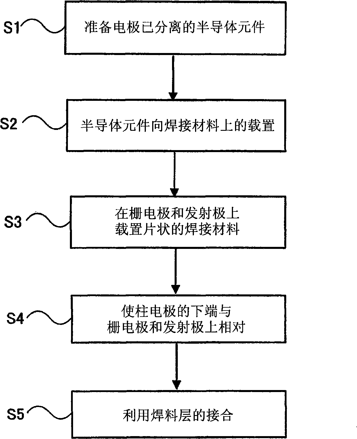
[0059] Hereinafter, the method of manufacturing the semiconductor device according to the first embodiment will be described in detail with reference to the drawings.
[0060] figure 1 It is a flowchart for explaining the manufacturing method of the semiconductor device of 1st Embodiment. In the manufacturing method of the semiconductor device according to the first embodiment, for example, a case where a vertical IGBT (Insulated Gate Bipolar Transistor: Insulated Gate Bipolar Transistor) element is used as a semiconductor element is exemplified. The semiconductor element used in the manufacturing method is not limited to the IGBT element.
[0061] First, prepare a semiconductor element (step S1), the semiconductor element is respectively provided with at least one gate electrode (first electrode) as a control electrode and an emitter electrode (second electrode) as a main electrode, and has a gate electrode (second electrode) configured to be connected to the gate electrode...
no. 2 approach
[0202] Next, use Figure 14 ~ Figure 19 A specific manufacturing method of the semiconductor device manufacturing method of the second embodiment will be described. In addition, in all the drawings shown below, the above-mentioned Figure 2 to Figure 13 The same symbols are assigned to the same components, and detailed description thereof will be omitted.
[0203] Figure 14 ~ Figure 19 It is a figure for demonstrating the manufacturing method of the semiconductor device of 2nd Embodiment.
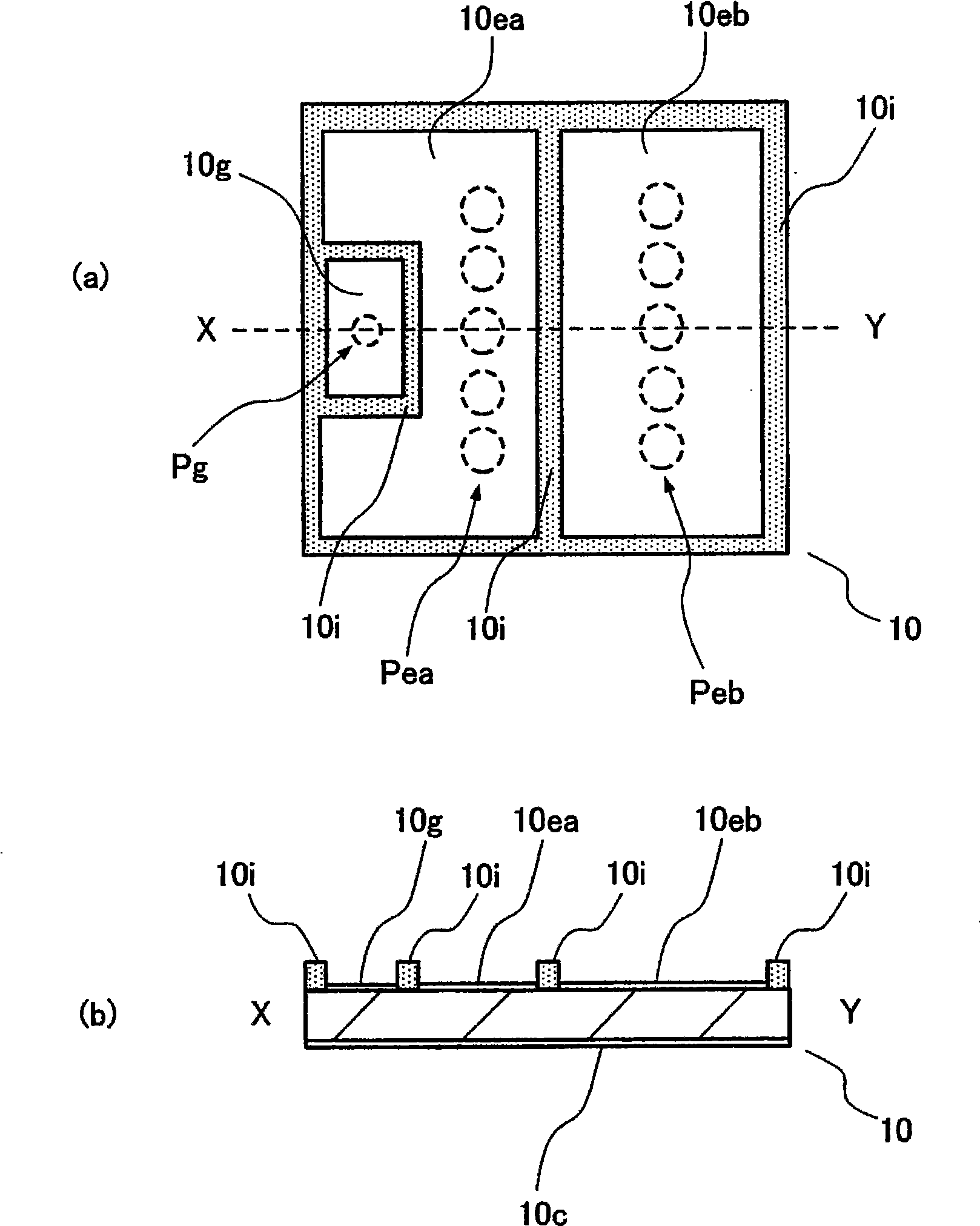
[0204] First, if Figure 14 As shown, semiconductor elements 10, 15 are prepared. These semiconductor elements 10 and 15 are fixed and supported by carbon fixing jigs (not shown).
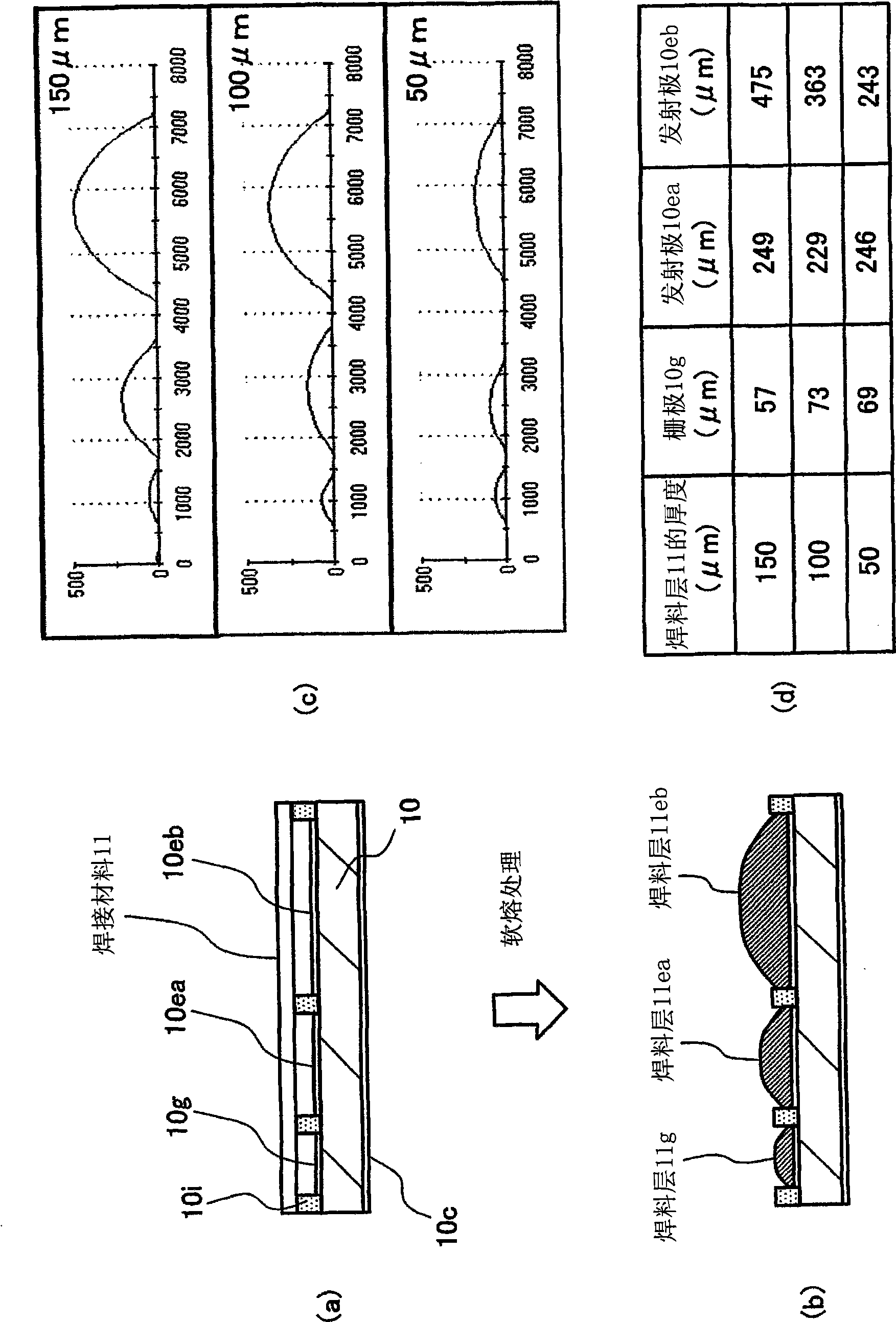
[0205]Next, the sheet-shaped solder material (first conductive bonding material) 11 is supported by the insulating layer 10i disposed on the upper surface side of the semiconductor element 10, so that the main surface of the solder material 11 faces the gate electrode 10g and the emitter electrodes 10ea, 1...
no. 3 approach
[0264] Next, use Figure 20 A specific manufacturing method of the semiconductor device manufacturing method of the third embodiment will be described. In addition, in all the drawings shown below, the above-mentioned Figure 2 to Figure 19 The same symbols are assigned to the same components, and detailed description thereof will be omitted.
[0265] Figure 20 Modifications of the semiconductor element 10 used in the method of manufacturing the semiconductor device according to the third embodiment are exemplified in FIG. here, Figure 20 (a), Figure 20 (b), Figure 20 (c), means along the figure 2 A cross-sectional view of the semiconductor element 10 at the position of the dotted line X—Y.
[0266] For example, the insulating layer 10i that separates the gate electrode 10g and the emitter electrode 10ea of the semiconductor element 10, or the insulating layer 10i between the emitter electrodes 10ea and 10eb, such as Figure 20 As shown in (a), it may be tapered...
PUM
Abstract
The invention provides a semiconductor device manufacturing method, which is object to improve the reliability and manufacture yield of the semiconductor apparatus. A semiconductor element has a first electrode and a second electrode separated by an insulation layer, a bonding material is configured on the metal foil, and the semiconductor element is placed on the bonding material in a mode of contacting it with a third electrode. In addition, the sheet-shape second conductive bonding material is opposite to the first electrode and the second electrode of the semiconductor element, and the lower end of the post electrode is opposite to the upper surfaces of the first electrode and the second electrode with bonding material intervening therebetween. And the welding material is separated byan insulation layer, the first electrode is connected to the post electrode through bonding material. Furthermore, the third electrode is jointed to the metal foil through bonding material. Therefore, the reliability and manufacture yield of the semiconductor apparatus can be improved.
Description
technical field [0001] The present invention relates to a method of manufacturing a semiconductor device, and more particularly to a method of manufacturing a semiconductor device on which a plurality of power semiconductor elements are mounted. Background technique [0002] In an inverter device, an uninterruptible power supply device, a machine tool, an industrial robot, etc., a semiconductor device mounted with a plurality of power semiconductor elements is used independently of its main device. Furthermore, recently, a semiconductor device of a wireless structure that does not use bonding wires has attracted attention in order to pass more large currents (for example, refer to Patent Document 1). [0003] Figure 21 It is a figure of main part of the semiconductor device of a wireless structure. [0004] The illustrated semiconductor device 100 has a metal base plate 101, an insulating plate 102 bonded to the metal base plate 101, and conductive patterns 103a, 103b, 103...
Claims
Application Information
Patent Timeline
Application Date:The date an application was filed.
Publication Date:The date a patent or application was officially published.
First Publication Date:The earliest publication date of a patent with the same application number.
Issue Date:Publication date of the patent grant document.
PCT Entry Date:The Entry date of PCT National Phase.
Estimated Expiry Date:The statutory expiry date of a patent right according to the Patent Law, and it is the longest term of protection that the patent right can achieve without the termination of the patent right due to other reasons(Term extension factor has been taken into account ).
Invalid Date:Actual expiry date is based on effective date or publication date of legal transaction data of invalid patent.

