Method for scanning keyboard scanning circuit

A scanning method and circuit technology, which is applied in the direction of electrical digital data processing, data processing input/output process, instruments, etc., can solve the problem of a large number of scanning ports for buttons, and achieve the effect of increasing the number and reducing the cost.

Inactive Publication Date: 2009-10-07
深圳市菉华半导体有限公司
View PDF0 Cites 4 Cited by
  • Summary
  • Abstract
  • Description
  • Claims
  • Application Information

AI Technical Summary

Problems solved by technology

[0004] In order to solve the technical problem that a large number of scanning ports are required when the number of keys is large in the prior art, the present invention proposes a scanning method for a keyboard scanning circuit that can save IO scanning ports

Method used


Image

  • Method for scanning keyboard scanning circuit
  • Method for scanning keyboard scanning circuit
  • Method for scanning keyboard scanning circuit

Examples


Embodiment Construction

[0017] The technical solutions of the present invention will be further described below in conjunction with the accompanying drawings and through specific embodiments.

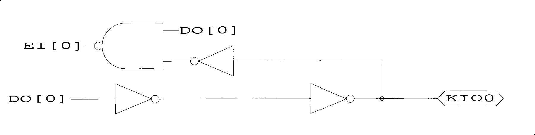
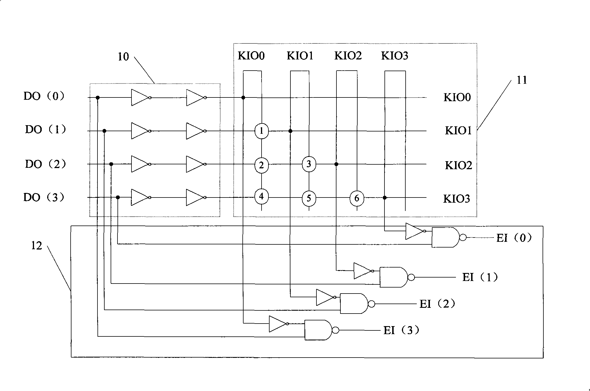
[0018] Such as figure 1 As shown, the scan signal DO(0) is output to KIO(0) after being inverted twice by two inverters. The output KIO(0) of the key scanning line is used as the input line and the output line of the key cross matrix at the same time. The output KIO(0) of the button scanning line passes through the inverter and then inputs a NAND gate together with the scanning signal DO(0), which outputs EI(0) as the judgment signal of the button action. The inverter far away from the scanning signal DO in each key scanning line is composed of a small-sized PMOS transistor and a large-sized NMOS transistor, and the output of the inverter constitutes the output KIO.

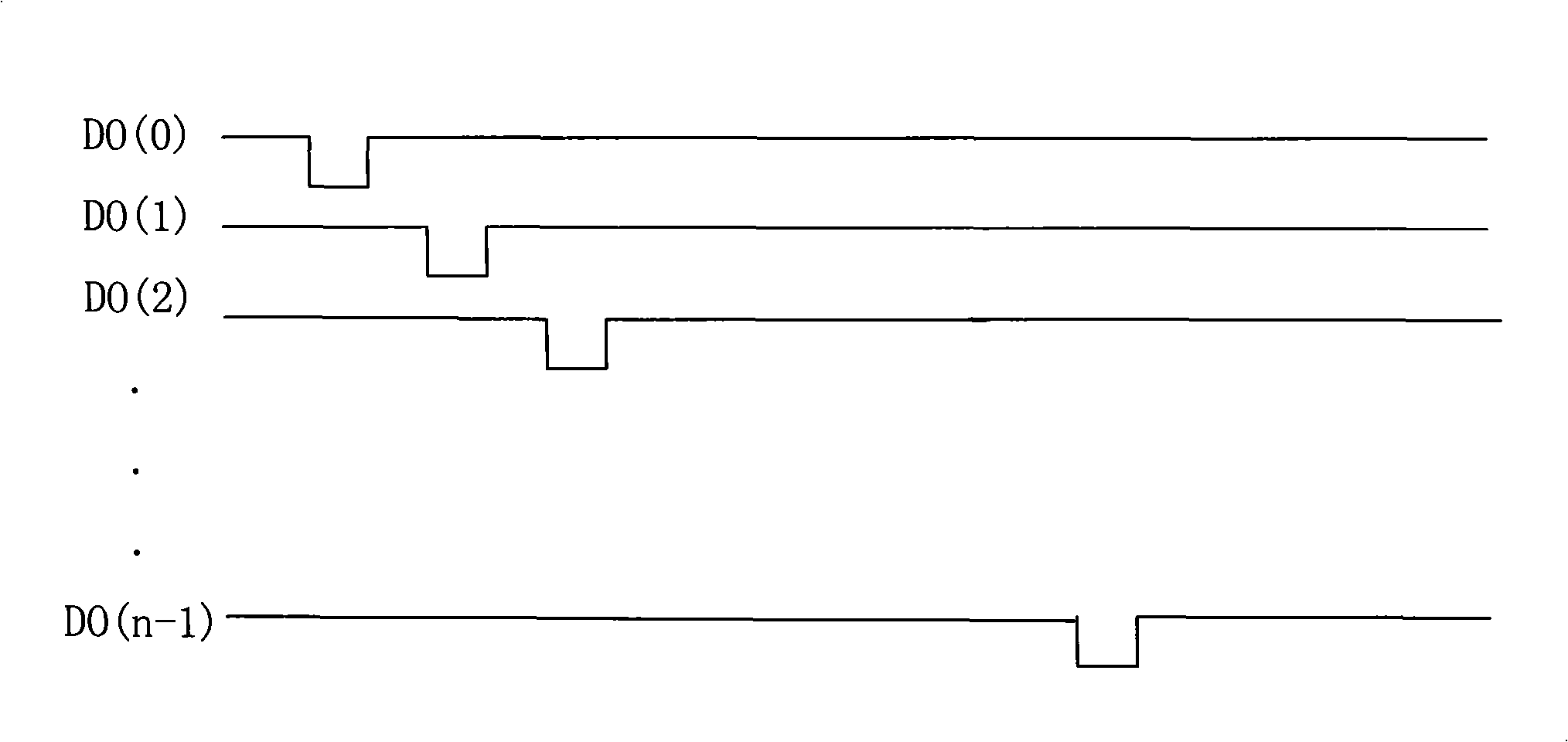
[0019] Such as figure 2 As shown, the scanning signal DO is a signal generated by the internal circuit, which is a low-level pulse and outpu...


PUM


Abstract

The invention discloses a keyboard scanning method, comprising following steps: outputting scanning signal of low level pulse; monitoring output level jumping state of key output lines, wherein only two outputs generate level jumping, the key is judged as a effective key. By the invention for N IO scanning interfaces, N*(N-1) / 2 keys can be composed, thereby greatly increasing number of keys and reducing producing cost.

Description

[0001] This application is a divisional application with the filing date of November 1, 2006, the application number of 200610063432.2, and the title of "Keyboard Scanning Circuit and Its Scanning Method". technical field [0002] The invention relates to a keyboard scanning method, in particular to a scanning method of a scanning circuit with a matrix structure. Background technique [0003] Existing keyboard scanning circuits mostly adopt a matrix structure, and each input and output line uses an IO scanning port. For an X*Y scanning matrix, that is, X scanning output lines, Y scanning input lines, and X scanning output lines The scanning signals are output to different Y scanning input lines in sequence, and the internal judgment circuit sends out different codes according to different combinations of output lines and input lines. Such as chip 3010, 64 keys need 16 IO scanning ports, 8 for input lines, the other 8 for output lines, chip 7461, 32 keys need 12 IO ports, 8 f...

Claims


Application Information

Patent Timeline
Patent Type & Authority Applications(China)
IPC IPC(8): H03M11/20G06F3/023
Inventor 金红志
Owner 深圳市菉华半导体有限公司
Why Eureka
Try Eureka