
Repairing method of photoresist pattern

A photoresist pattern and photoresist technology, applied to the photoplate making process of the pattern surface, the original for photomechanical processing, optics, etc., can solve the problems of increasing production cost, low production efficiency, and consumption

Inactive Publication Date: 2009-10-28
CONTREL TECH CO LTD
View PDF0 Cites 11 Cited by
  • Summary
  • Abstract
  • Description
  • Claims
  • Application Information

AI Technical Summary

Problems solved by technology

[0005] However, after the etching of the circuit structure is completed, the repair method of soldering additional metal circuits generally requires the use of expensive equipment and some related consumables, which will greatly increase the production cost
In addition, such a repair method will also take a long time, resulting in low production efficiency

Method used


Image

  • Repairing method of photoresist pattern
  • Repairing method of photoresist pattern
  • Repairing method of photoresist pattern

Examples


Embodiment Construction

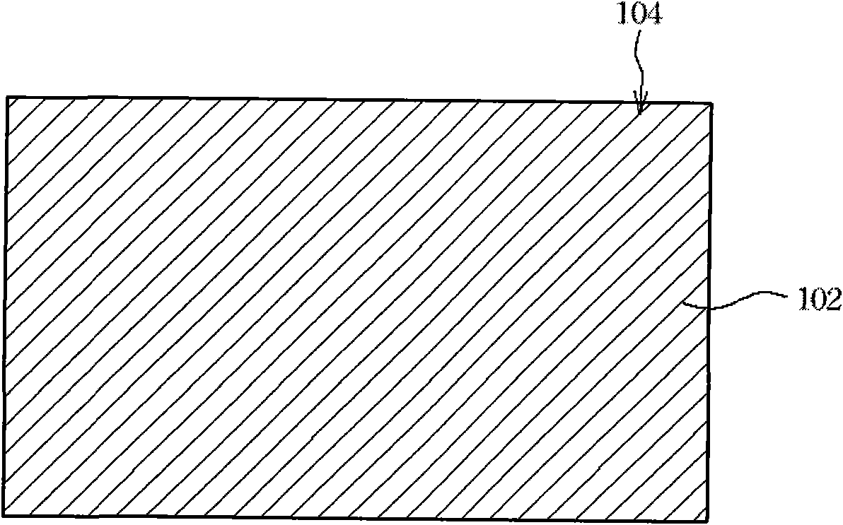
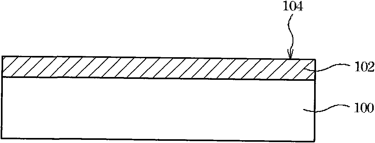
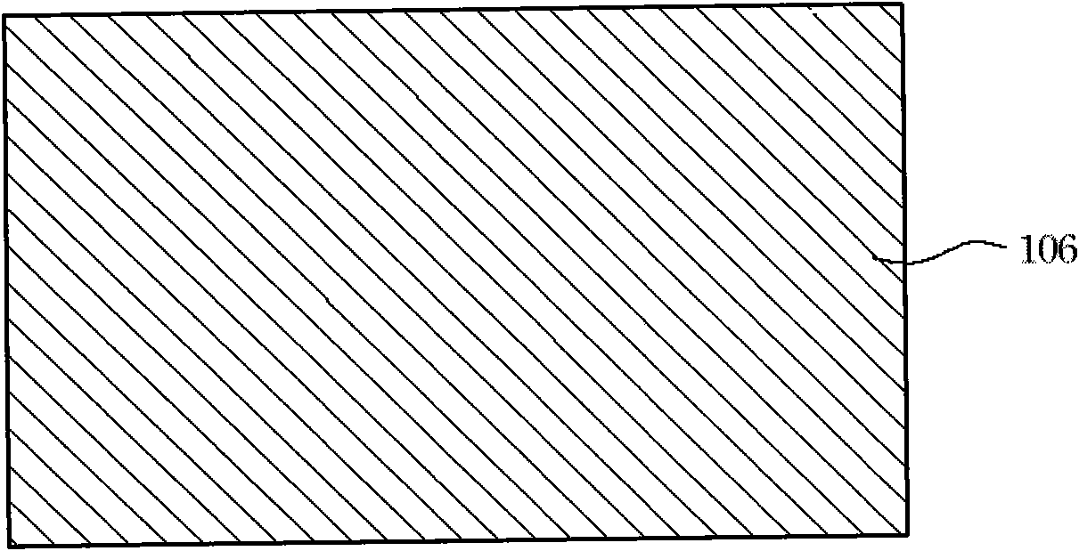
[0020] The invention discloses a method for repairing a photoresist pattern. In order to make the description of the present invention more detailed and complete, reference may be made to the following description in conjunction with the accompanying drawings Figure 1A to Figure 6B .

[0021] Please refer to Figure 1A to Figure 5B , which shows a process diagram of a method for repairing a photoresist pattern according to a preferred embodiment of the present invention, wherein Figure 1A , Figure 2A , Figure 3A , Figure 4A and Figure 5A for the top view, and Figure 1B , Figure 2B , Figure 3B , Figure 4B and Figure 5B respectively Figure 1A , Figure 2A , Figure 3A , Figure 4A and Figure 5A sectional view. In an exemplary embodiment, when performing the photoresist pattern repairing process, a substrate 100 is provided first, wherein the substrate 100 preferably has a flat surface for device structures to be disposed thereon. The substrate 100 ca...


PUM


Abstract

The invention discloses a repairing method of a photoresist pattern, which at least comprises the following steps: a material layer is formed on a substrate; a photoresist pattern is formed on the first part of the surface of the material layer, wherein the photo-etching glue pattern at least comprises a defect area exposed out of the second part of the surface of the material layer; and a repairing step is carried out to form a photo-etching glue layer which is arranged in the defect area of the photo-etching glue pattern and covers the second part of the surface of the material layer.

Description

technical field [0001] The invention relates to a method for repairing a photoresist pattern, and in particular to a method for repairing a photoresist pattern that can be performed in real time. Background technique [0002] At present, in the process of manufacturing multiple sets of substrates for thin film transistors of liquid crystal displays, it is common to deposit material films first, and then use photolithography, etching and other processes to produce multiple sets of patterns. In the photolithography process, a photoresist layer is first coated on the material film, and then the photoresist layer is exposed through a photomask to transfer the photomask pattern to the photoresist layer, followed by development to remove part of the photoresist layer to transfer the photomask pattern to the photoresist layer, and then bake the remaining photoresist layer to complete the fabrication of the photoresist pattern. [0003] After the photolithography process is complet...

Claims


Application Information

Patent Timeline
Patent Type & Authority Applications(China)
IPC IPC(8): G03F1/00G03F1/72
Inventor 简永杰江鸿儒
Owner CONTREL TECH CO LTD
Learn More