Control scanning circuit of raster optical modulator projection device

A technology for light modulators and projection devices, which is applied in instruments, televisions, optics, etc., can solve the problems of reducing the signal transmission rate of the system circuit, increasing the complexity and interference of the connection of peripheral circuit modules, and reducing the dynamic response time. requirements, rich grayscale color modulation, the effect of eliminating cross effects

Inactive Publication Date: 2011-11-09
CHONGQING UNIV
View PDF2 Cites 0 Cited by
  • Summary
  • Abstract
  • Description
  • Claims
  • Application Information

AI Technical Summary

Problems solved by technology

If the peripheral drive circuit is packaged separately from the active matrix, this will increase the signal noise interference of each circuit module due to the interconnection, reduce the signal transmission rate of the system circuit, and for the projection display of the grating light modulator with a large area array , it is necessary to lead out thousands of input pin ports, these pins not only occupy a large area, increase the cost, but also increase the complexity of the connection between peripheral circuit modules, which limit the real high resolution of the grating optical modulator , high-definition projection display
[0003] The Chinese Invention Patent Application Publication No. CN 101382655A discloses an active matrix-driven grating light modulator, but currently there is no projecting device for the active matrix-driven grating light modulator in the prior art. control scan circuit

Method used


Image

  • Control scanning circuit of raster optical modulator projection device
  • Control scanning circuit of raster optical modulator projection device
  • Control scanning circuit of raster optical modulator projection device

Examples


Embodiment Construction

[0023] Hereinafter, preferred embodiments of the present invention will be described in detail with reference to the accompanying drawings.

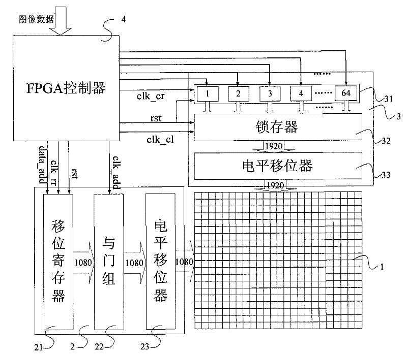
[0024] see figure 1 , the control scanning circuit of the grating light modulator projection device is used to drive the pixel array composed of M columns×N rows of grating light modulators, and the control scanning circuit of the grating light modulator projection device with 1920×1080 resolution is taken as an example. Note that the resolution grating light modulator projection device has a pixel array composed of 1920 rows×1080 columns of grating light modulators.

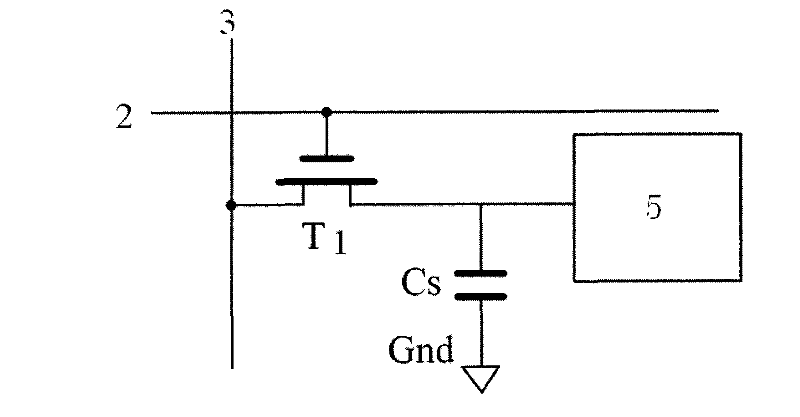
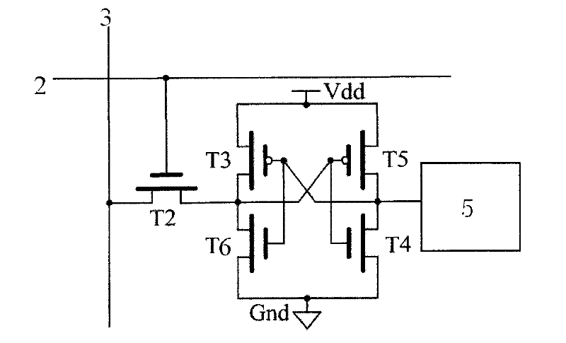
[0025] The control scanning circuit of the grating light modulator projection device is formed by monolithic packaging of an active matrix drive circuit 1, a row drive circuit 2, and a column drive circuit 3, and the control of the active matrix can be realized through several control signals and data buses. control, so as to realize the high-definition and high-resolutio...


PUM


Abstract

The invention provides a control scanning circuit of raster optical modulator projection device, which realizes high-resolution, high-definition projection display of the raster optical modulator. Thecontrol scanning circuit of raster optical modulator projection device is used for driving the pixel array composed of M row*N line optical modulators, comprising an active matrix drive circuit composed of M*N active matrix drive units, capable of controlling the pressure of the raster optical modulator to modulate the light based on the control signal and the image signal; a first driving circuit capable of receiving the control signal sent from the control device to gate the raster optical modulator on the same straight; and a second drive circuit capable of receiving the control signal andthe image signal sent from the control device to output the image data to the gated raster optical modulator.

Description

technical field [0001] The invention relates to a control scanning circuit of a display device, in particular to a control scanning circuit of a grating light modulator. Background technique [0002] The Chinese Invention Patent Application Publication No. CN1658009A discloses a grating light modulator and its array. The processing of the grating light modulator is simpler than that of DMD, and at the same time, it solves the disadvantage that GLV is difficult to form an area array. For the projection display of the small area grating light modulator, it can be realized by using the passive matrix driver. However, for the projection display of larger area grating light modulators, it is difficult to achieve high-quality image display due to the cross effect of passive matrix driving. And using the active matrix to drive the grating light modulator can make the grating light modulator really face high-definition and high-resolution projection display. If the peripheral driv...

Claims


Application Information

Patent Timeline
Patent Type & Authority Patents(China)
IPC IPC(8): G09G3/36H04N5/74G02B26/08
Inventor 温志渝金珠张智海张洁
Owner CHONGQING UNIV
Why Eureka
Try Eureka