A method of producing solid-state imaging device

A solid-state imaging device and solid-state imaging technology are applied in radiation control devices, semiconductor/solid-state device parts, electric solid-state devices, etc., which can solve problems such as poor flatness, inability to guarantee stiffness, narrow distance, etc., and achieve improved reliability. Transferability, improvement of stiffness, and damage prevention effect

Inactive Publication Date: 2009-10-28
FUJIFILM CORP
View PDF3 Cites 15 Cited by
  • Summary
  • Abstract
  • Description
  • Claims
  • Application Information

AI Technical Summary

Problems solved by technology

[0004] In such a method of manufacturing a solid-state imaging device, particularly in the dicing process, there is a problem that the solid-state imaging element wafer is damaged by fragments of the light-transmitting substrate generated at the time of dicing, because the light-transmitting substrate and the solid-state imaging The distance between the gaps formed between element wafers is narrow
For this reason, the light-transmissive substrate in which the channels are arranged between the spacers cannot ensure sufficient stiffness, which causes problems in that the light-transmissive substrate bends at the time of bonding to deteriorate flatness, and at the time of transfer Bending, whereby light transmissive substrates cannot be handled or damaged

Method used


Image

  • A method of producing solid-state imaging device
  • A method of producing solid-state imaging device
  • A method of producing solid-state imaging device

Examples


Embodiment

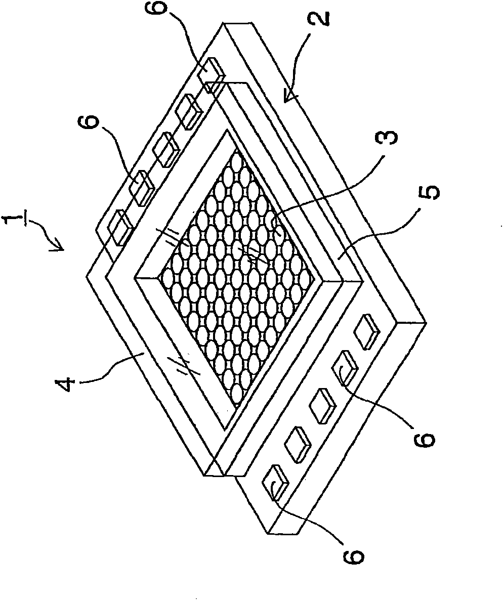
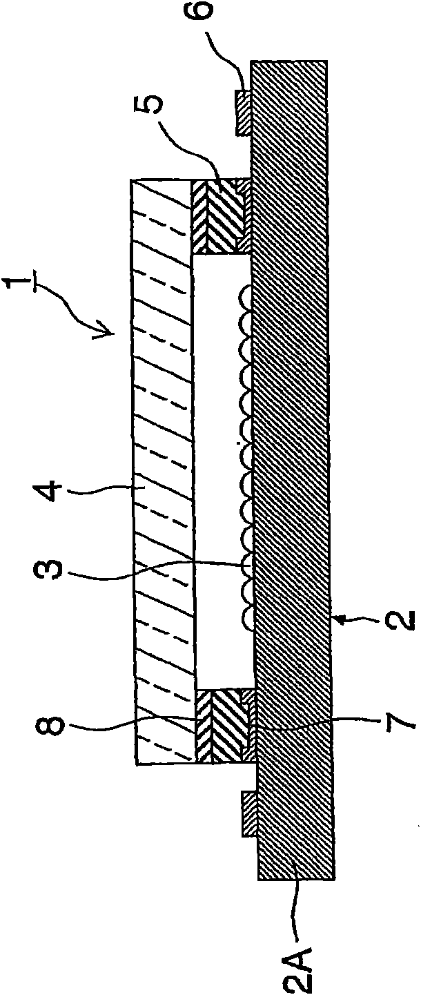
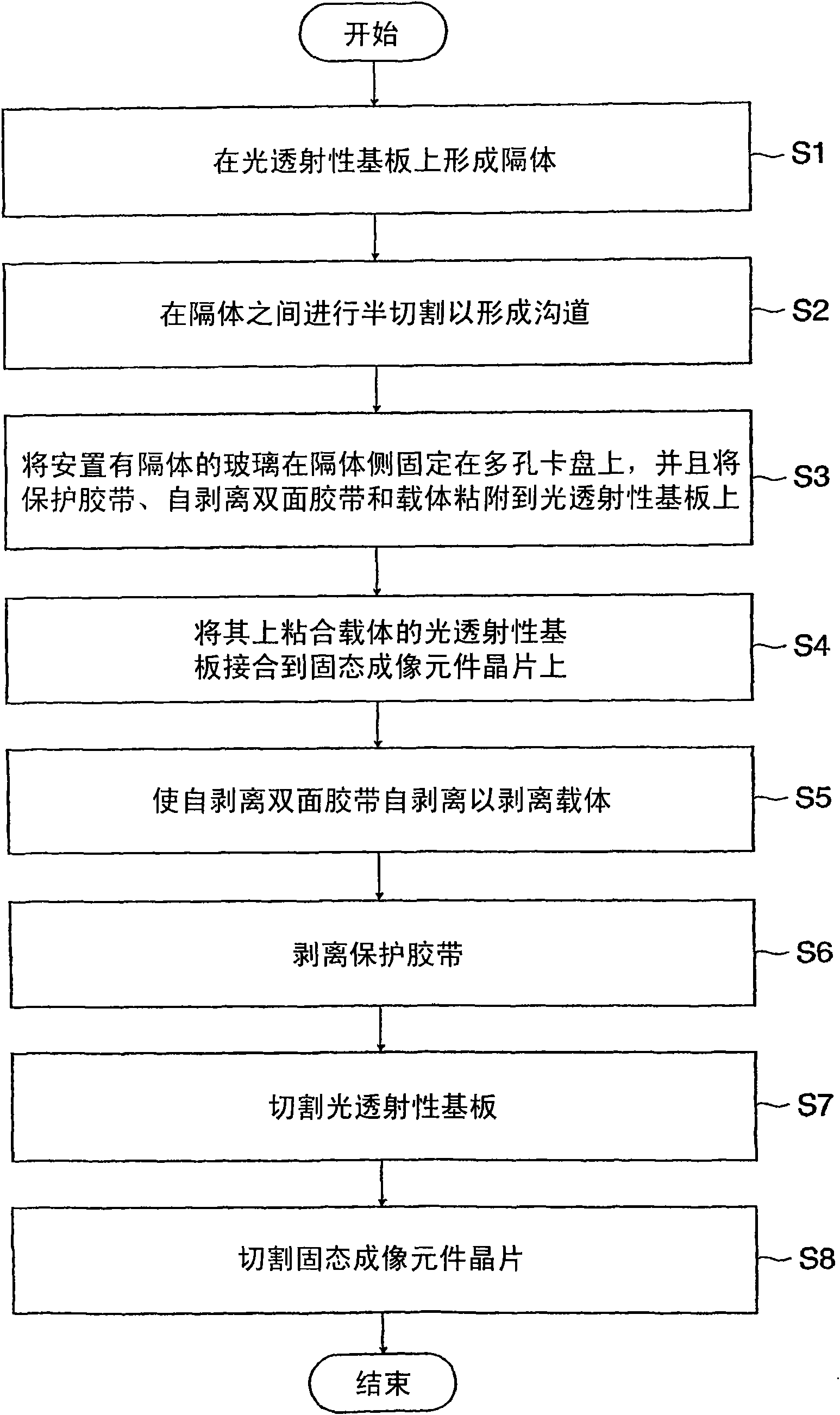
[0097] A specific example of a method of manufacturing a solid-state imaging device according to the present invention is described below. The reference numbers appearing below are used in figure 1 , 2 , 4 and those shown in 6.

[0098] Pyrex (registered trademark) glass of 8 inches and 300 μm thick was used as the light-transmitting substrate 10 . Spacers 5 having a height of 50 μm are formed on the light-transmitting substrate 10 .

[0099] Between the spacers 5, half-cut cutting was performed with a depth of 150 μm and 80 lines in the vertical and horizontal directions. A cutting device produced by DISCO Corporation was used for cutting. "UHP-1005M3 (ultraviolet peeling type)" manufactured by DENKIKAGAKU KOGYO KABUSHIKI KAISHA was used as a dicing tape. A resin-bonded grinding stone with an outer diameter of 55 mm, a width of 0.1 mm to 0.7 mm, and a grain size of #400 was used. The number of revolutions of the grindstone was 30000 rpm and the processing speed was 1 mm...


PUM


Abstract

A method of producing a solid-state imaging device according to one embodiment of the present invention is characterized in that, in a method of producing a solid-state imaging device such that a solid-state imaging element wafer is bonded to a light transmissive substrate on one surface of which spacers are formed so as to surround solid-state imaging elements formed on the solid-state imaging element wafer and ditches are formed between the spacers to produce a bonded substrate and then the bonded substrate is divided correspondingly to the individual solid-state imaging elements, a support is bonded to the surface opposite to the surface of the light transmissive substrate on which the ditches are formed.

Description

technical field [0001] The present invention relates to a method of manufacturing a solid-state imaging device, in particular, to a method of manufacturing a solid-state imaging device by bonding a solid-state imaging element wafer to a light-transmitting substrate. Background technique [0002] In recent years, solid-state imaging devices formed of charge-coupled devices (CCD) or complementary metal-oxide semiconductors (CMOS) used in digital cameras or cellular phones have been required to be further miniaturized and mass-produced. [0003] In order to miniaturize and mass-produce a solid-state imaging device based on these requirements, a solid-state imaging device manufactured such that a plurality of solid-state imaging devices are formed thereon and a method of manufacturing the same have been proposed. The solid-state imaging element wafer of the light-receiving unit is bonded to the light-transmitting substrate via spacers formed corresponding to positions surroundin...

Claims


Application Information

Patent Timeline
Patent Type & Authority Applications(China)
IPC IPC(8): H01L27/14H01L23/02H01L31/02
CPCH01L27/14632H01L27/14618H01L27/14687H01L31/0203H01L24/94H01L27/146
Inventor 渡边万次郎
Owner FUJIFILM CORP
Why Eureka
Try Eureka