Power module with lower stray inductance

A power module and stray inductance technology, applied in the field of power electronics, can solve problems such as excessive parasitic inductance, and achieve the effect of small parasitic inductance and low voltage stress

Active Publication Date: 2009-11-18
STARPOWER SEMICON
View PDF0 Cites 10 Cited by
  • Summary
  • Abstract
  • Description
  • Claims
  • Application Information

AI Technical Summary

Problems solved by technology

[0006] The invention aims to solve the problem of excessive parasitic inductance in the existing power module

Method used


Image

  • Power module with lower stray inductance
  • Power module with lower stray inductance
  • Power module with lower stray inductance

Examples


Embodiment Construction

[0015] The present invention will be further described in conjunction with the accompanying drawings and embodiments.

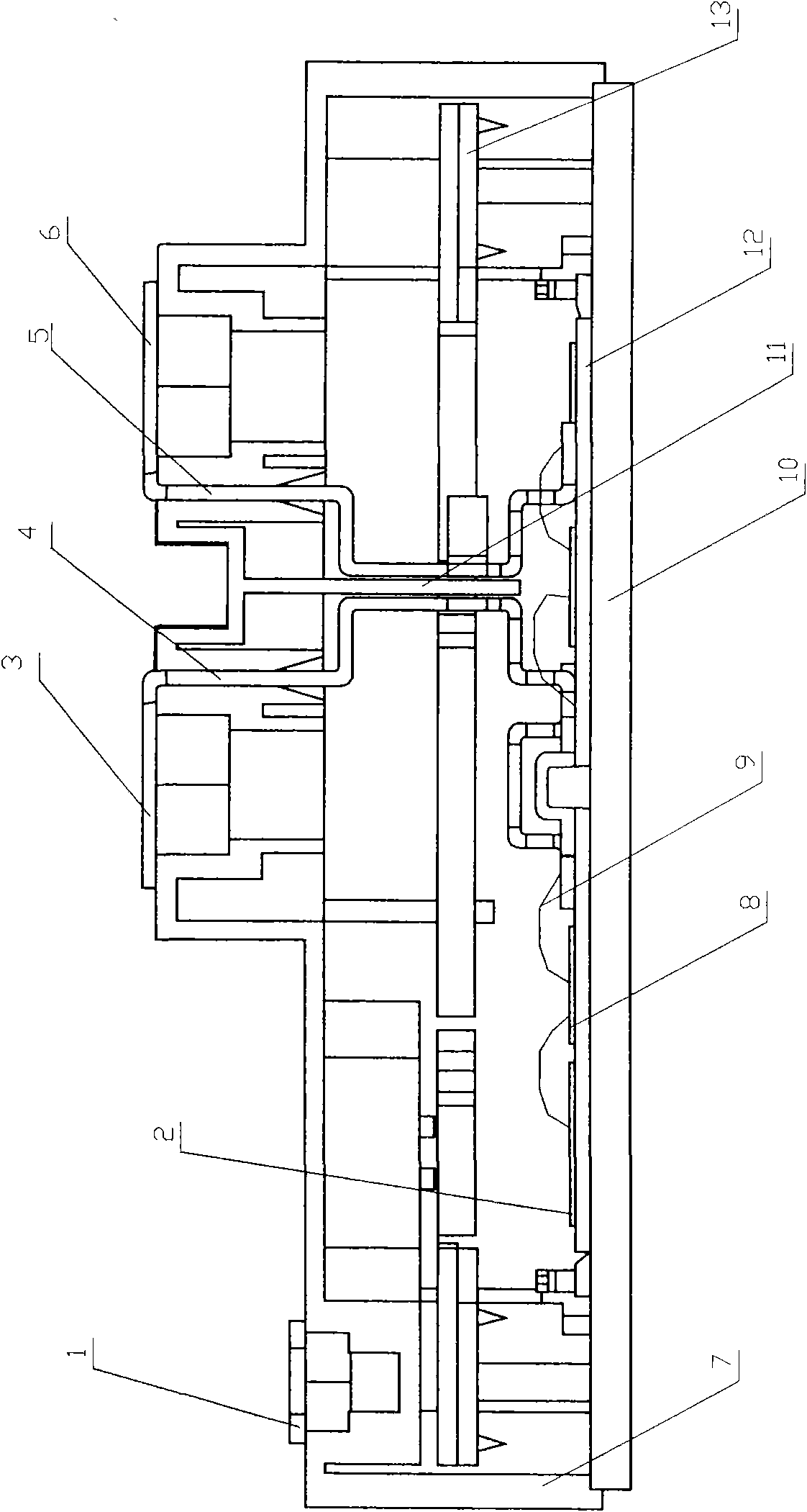
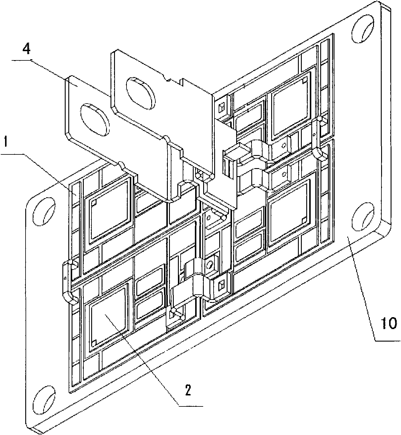
[0016] The power module in this embodiment is an insulated gate bipolar transistor (IGBT) module. Such as Figure 1 to Figure 5 As shown, the power module includes an insulated gate bipolar transistor chip 2, a diode chip 8, an insulating substrate (DBC) 12, a heat dissipation plate 10, a bonding aluminum wire 9, a power terminal 4 and a power terminal 5, a bracket 13, and a signal terminal 1 and housing 7. The insulating substrate 12 is located on the heat sink 10 , and the IGBT chip 2 and the diode chip 8 are soldered to the insulating substrate 12 by reflow.

[0017] The power module 15 is provided with a power terminal 4 and a power terminal 5, which are respectively connected to the positive pole (P) 3 of the busbar and the negative pole (N) 6 of the busbar, and the two are connected to the power terminal 4 and the power terminal 5 on the busbar. 5 ad...


PUM


Abstract

The invention discloses a power module with lower stray inductance. The power module comprises a chip, an insulating substrate, a radiating rib and power terminals, wherein the insulating substrate is positioned on the radiating rib; the chip is welded on the insulating substrate; at least two power terminals are arranged in the module and are connected to the positive electrode and the negative electrode of a direct current bus respectively; and the two power terminals connected to the direct current bus are of a stacked bus structure. The power module has the characteristics of small stray inductance, small voltage stress endured when the module is turned off.

Description

technical field [0001] The invention belongs to the field of power electronics and relates to a power module, specifically a power module with relatively low stray inductance. Background technique [0002] Power modules include insulated gate bipolar transistor (IGBT) modules, diode modules, MOSFET modules, intelligent power (IPM) modules, etc. Due to structural design problems of power terminals in these existing power modules, there is a relatively high parasitic inductance inside the module, so that the module bears a relatively large voltage stress when it is turned off. [0003] Now take an insulated gate bipolar transistor (IGBT) module as an example to explain how to withstand a large voltage stress when it is turned off due to the existence of high parasitic inductance. The insulated gate bipolar transistor (IGBT) module is a new type of power electronic device, which has both the input characteristics of MOSFET and the output characteristics of BJT, and it bears a ...

Claims


Application Information

Patent Timeline
Patent Type & Authority Applications(China)
IPC IPC(8): H01L25/00H01L23/48H01L23/12
CPCH01L2924/0002
Inventor 刘志宏朱翔李冯沈华
Owner STARPOWER SEMICON
Why Eureka
Try Eureka