Gallium arsenide PIN diode and preparation method thereof

A manufacturing method and diode technology, applied in the field of diodes, can solve problems such as easy collapse or breakage of the bridge surface, increase process difficulty, and reduce yield rate, etc., and achieve the effects of easy monolithic integration, simple process, and reduced parasitic capacitance

Active Publication Date: 2008-03-12
北京中科微投资管理有限责任公司
View PDF0 Cites 12 Cited by
  • Summary
  • Abstract
  • Description
  • Claims
  • Application Information

AI Technical Summary

Problems solved by technology

[0009] However, the air bridge structure will increase the difficulty of the process, and the bridge deck is prone to collapse or fracture, reducing the yield, and the bridge deck metal will introduce a certain amount of parasitic inductance

Method used


Image

  • Gallium arsenide PIN diode and preparation method thereof
  • Gallium arsenide PIN diode and preparation method thereof
  • Gallium arsenide PIN diode and preparation method thereof

Examples


Embodiment Construction

[0040] In order to make the objectives, technical solutions, and advantages of the present invention clearer, the following further describes the present invention in detail in conjunction with specific embodiments and with reference to the accompanying drawings.

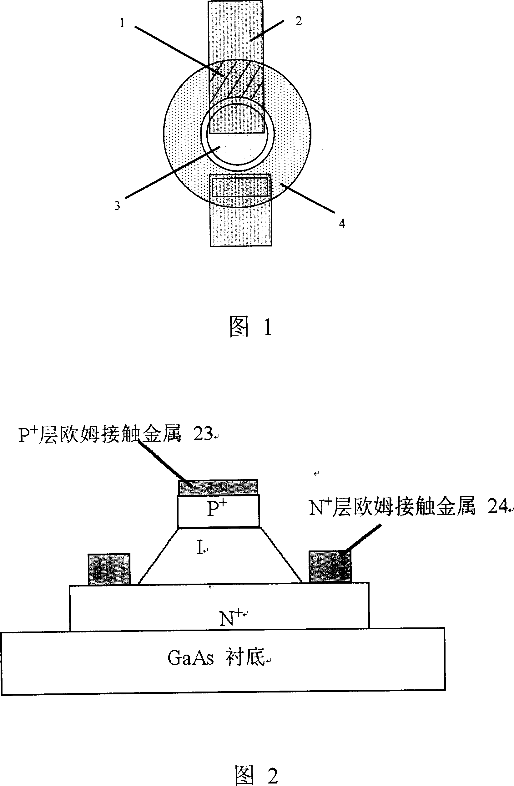
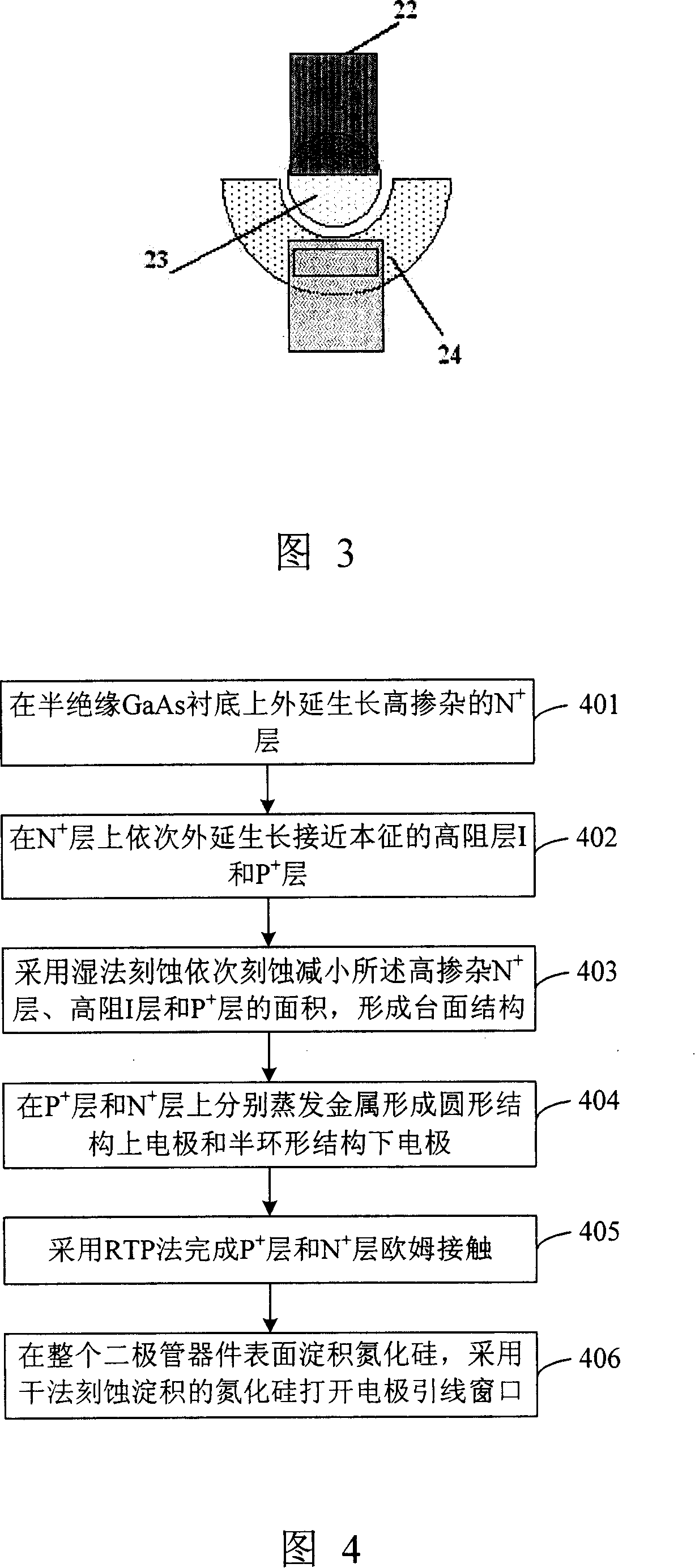
[0041] As shown in Figure 2, Figure 2 is a cross-sectional view of the GaAs PIN diode provided by the present invention. The cross-sectional view is a cross-sectional view perpendicular to the substrate along the two ends of the lower electrode half ring of the GaAs PIN diode. The GaAs PIN diode includes:

[0042] Semi-insulating GaAs substrate used to support the entire GaAs PIN diode;

[0043] Highly doped N epitaxially grown on semi-insulating GaAs substrate + Layer, in highly doped N + The high-resistance I layer and P layer that are close to intrinsic and epitaxially grown on the layer + Layer; by using wet etching, the highly doped N + Layer, high resistance I layer and P + The area of ​​the layer is successively ...


PUM

PropertyMeasurementUnit
radiusaaaaaaaaaa
radiusaaaaaaaaaa

Abstract

The invention discloses a GaAs PIN diode, which comprises: a semi-insulating GaAs underlay for supporting the whole GaAs diode; a high doped layer N growing in extension on the semi-insulating GaAs underlay, resistive formations I and P close to eigen growing in extension in turn on the high doped layer N; By wet process and etching, the areas of the said high doped layer N, resistive formations I and P reduced in turn to form a mesa structure; a top electrode of the round structure formed by metal evaporator on layer P; a semi-orbicular bottom electrode formed by metal evaporator on layer N. The invention also discloses a manufacturing method of GaAs PIN diode. The invention efficiently lowers the parasitic capacitance of the PIN diode without increasing the difficulty of the process and simultaneously greatly shortens the microstrip line connected with the top electrode. The spurious inductance brought by the invention can be greatly reduced or even omitted without using the air-bridge process. The invention has the advantages of easy making, better high frequency characteristic, which is easy to realize the single scale integration.

Description

Technical field [0001] The invention relates to the technical field of diodes in microelectronic devices, in particular to a gallium arsenide (GaAs) PIN diode and a manufacturing method thereof. Background technique [0002] PIN diode is the most commonly used device in microwave control circuits. It is characterized by high controllable power, low insertion loss, and good characteristics of approximate short circuit and open circuit. It can be used in switching circuits, limiters, and phase shifters. , Attenuators and modulators and other control circuits. [0003] Compared with traditional Si PIN diodes, GaAs PIN diodes have superior high-frequency characteristics and are indispensable and important devices in microwave systems. Therefore, it is of great significance to develop GaAs PIN diodes with excellent performance. [0004] As shown in Figure 1, Figure 1 is a top view of a common mesa PIN diode. Among them, the upper electrode 3 and the lower electrode 4 are respectively ...

Claims


Application Information

Patent Timeline
Patent Type & Authority Applications(China)
IPC IPC(8): H01L29/868H01L21/329
Inventor 杨浩张海英吴茹菲
Owner 北京中科微投资管理有限责任公司
Why Eureka
Try Eureka