Ultra-broadband differential voltage probes

a differential voltage and probe technology, applied in the field of wideband differential voltage probes, can solve the problems of affecting the accuracy of measurement results, so as to minimize parasitic inductance and capacitance, and maximize the amount of power carried

Active Publication Date: 2005-11-17
APTIV TECH LTD
View PDF10 Cites 13 Cited by
  • Summary
  • Abstract
  • Description
  • Claims
  • Application Information

AI Technical Summary

Benefits of technology

[0016] Advantageously, the present invention provides a low-cost ultra-broadband probe having an extremely flat response characteristic over a frequency range of approximately 0 to at least 1.5 gigahertz. The probe may be ...

Problems solved by technology

Floating the ground of either the circuit under test or the signal analysis device may open the ground loop; however, floating the ground may result in an electrical shock hazard as one of the devices no longer has a connection to ground through which an electrical short could be carried.
Another problem with probes, including high impedance FET probes, relates to input impedance.
While some conventional passive probes utilize a high input impedance, for example 10 megohms in parallel with 10 picofarads, such probes are not high impedance at higher frequencies and generally have significant measurement error at higher frequencies because of the resonance generated between the p...

Method used


Image

  • Ultra-broadband differential voltage probes
  • Ultra-broadband differential voltage probes
  • Ultra-broadband differential voltage probes

Examples


Embodiment Construction

[0027] The embodiment disclosed below is not intended to be exhaustive or limit the invention to the precise forms disclosed in the following detailed description. Rather, the embodiment is chosen and described so that others skilled in the art may utilize its teachings.

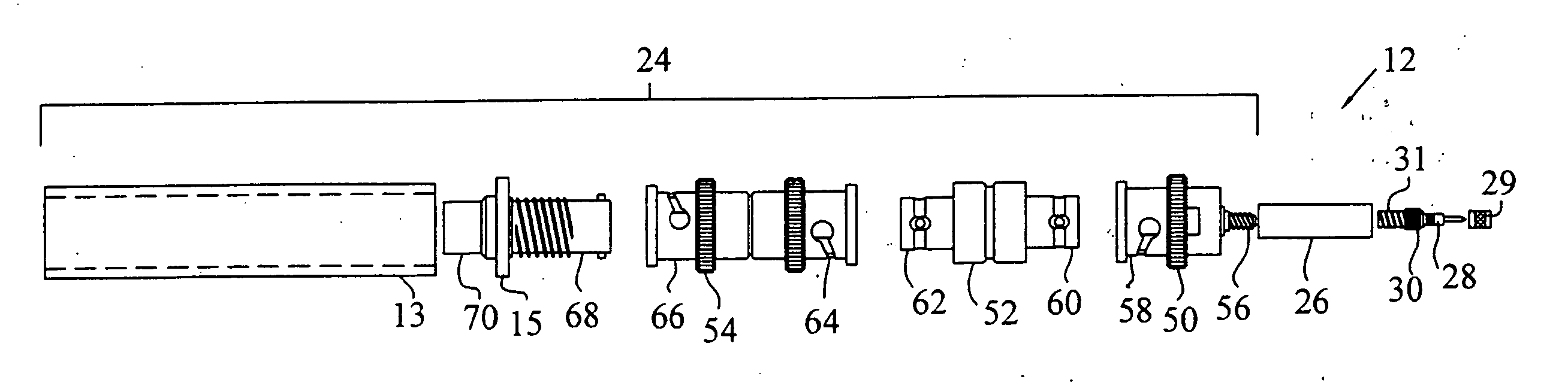
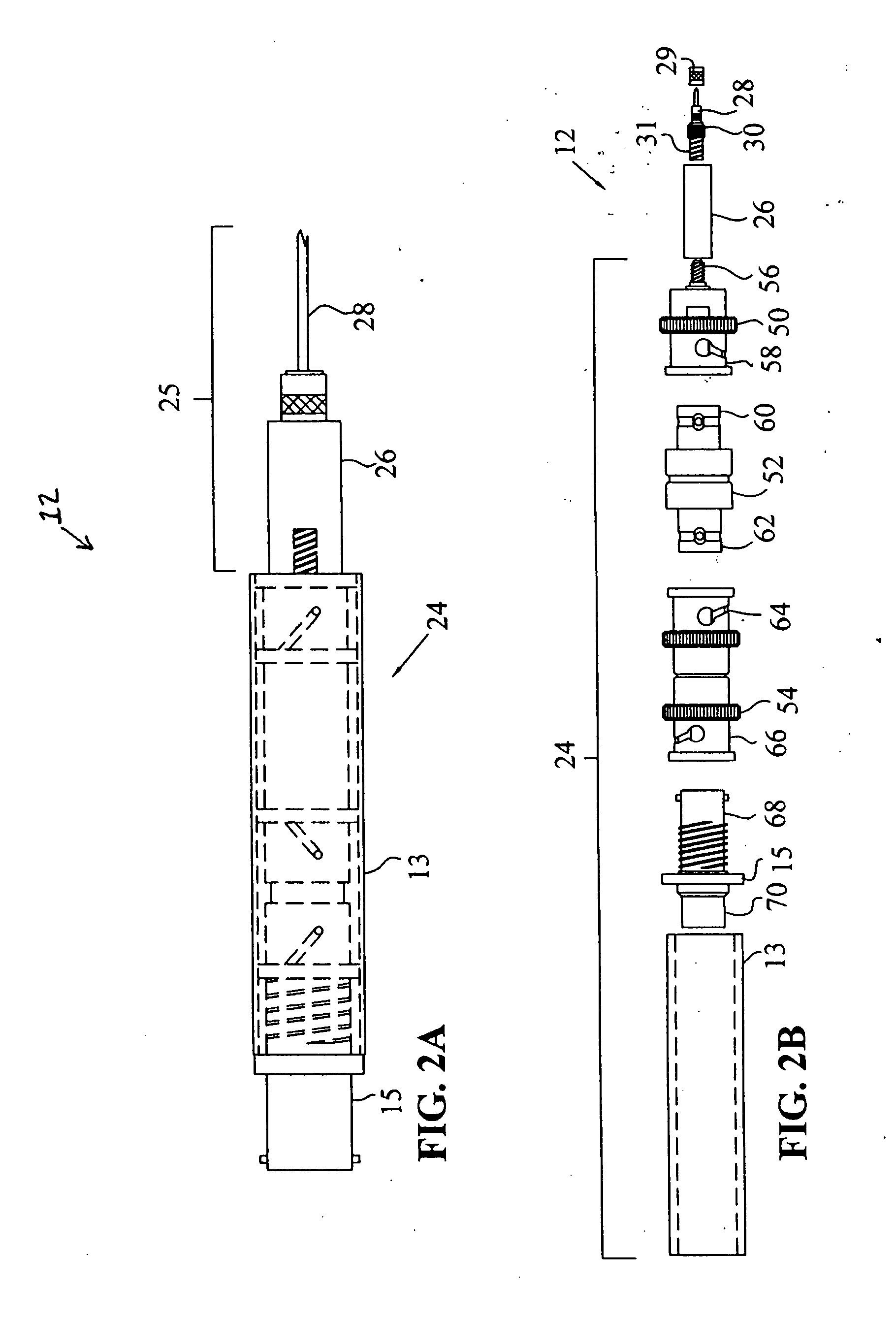
[0028] Referring to FIG. 3, balanced probe pair assembly 10 includes probes 12, coaxial cables 14, and may include ground lead 16. Assembly 10 may be coupled to input channel connector 22 of signal analysis device 18 using, for example, combiner 20. Referring to FIG. 2A, each probe 12 includes probe body 24, probe end 25, body sleeve 13, and base connector 15.

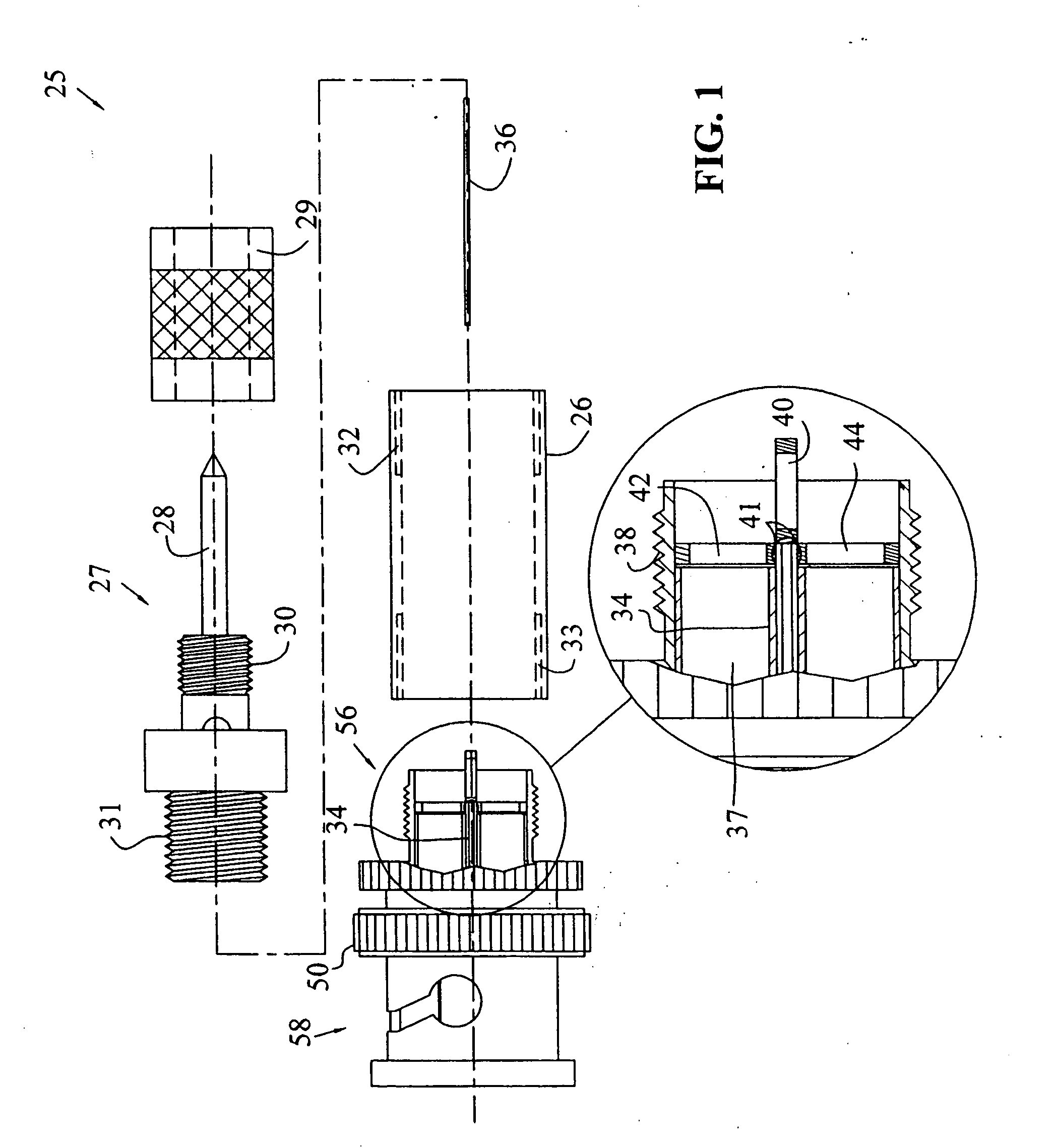
[0029] Referring to FIG. 1, each probe end 25 includes probe tip sleeve 26 coupling probe end connector 50 and probe tip 27. Probe tip 27 includes elongate tip 28, threaded sleeve 29, distal tip thread 30, and proximate tip thread 31. Threaded sleeve 29 engages distal tip thread 30 and proximate tip thread 31 engages distal sleeve thread 32 of probe tip sleeve...


PUM


Abstract

Passive balanced probes are disclosed for use with a signal analysis device. The probes are very low cost relative to typical commercially available probes and provide an extremely flat response over a frequency range of approximately 0 to at least 1.5 gigahertz. The probes include a probe body constructed primarily from conventional components, a first surface mount resistor electrically connected between a probe tip and a center conductor, and two surface mount resistors electrically connected and parallel between the center conductor and a conductive shield. The probes further include a coaxial cable for connection to an instrument combiner or other instrument connection device.

Description

TECHNICAL BACKGROUND [0001] The present invention generally relates to high frequency measurement equipment, and, more particularly, the invention relates to wideband differential voltage probes. BACKGROUND OF THE INVENTION [0002] Oscilloscopes, spectrum analyzers, and other signal analysis devices are generally used to measure a voltage signal between two points with one of the points often being referenced to earth ground. However, in many cases it is advantageous to measure the voltage between two points in a circuit with neither of the points being the ground to which the signal analysis device is referenced. [0003] If the ground of the signal analysis device is connected to the ground of the circuit under test, a ground loop may result. The ground loop may act as a secondary transformer winding, thus producing a magnetic field and creating a signal in nearby conductors, such as the probe used to connect the signal analysis device with the circuit under test. Additionally, curre...

Claims


Application Information

Patent Timeline
IPC IPC(8): G01R1/067G01R31/02
CPCG01R1/06788G01R1/06772
Inventor CAPPS, CHARLES P.JOHNSON, BRIAN W.GLOUDEMANS, JEFFREY M.LANE, JOHN A.
Owner APTIV TECH LTD
Why Eureka
Try Eureka