

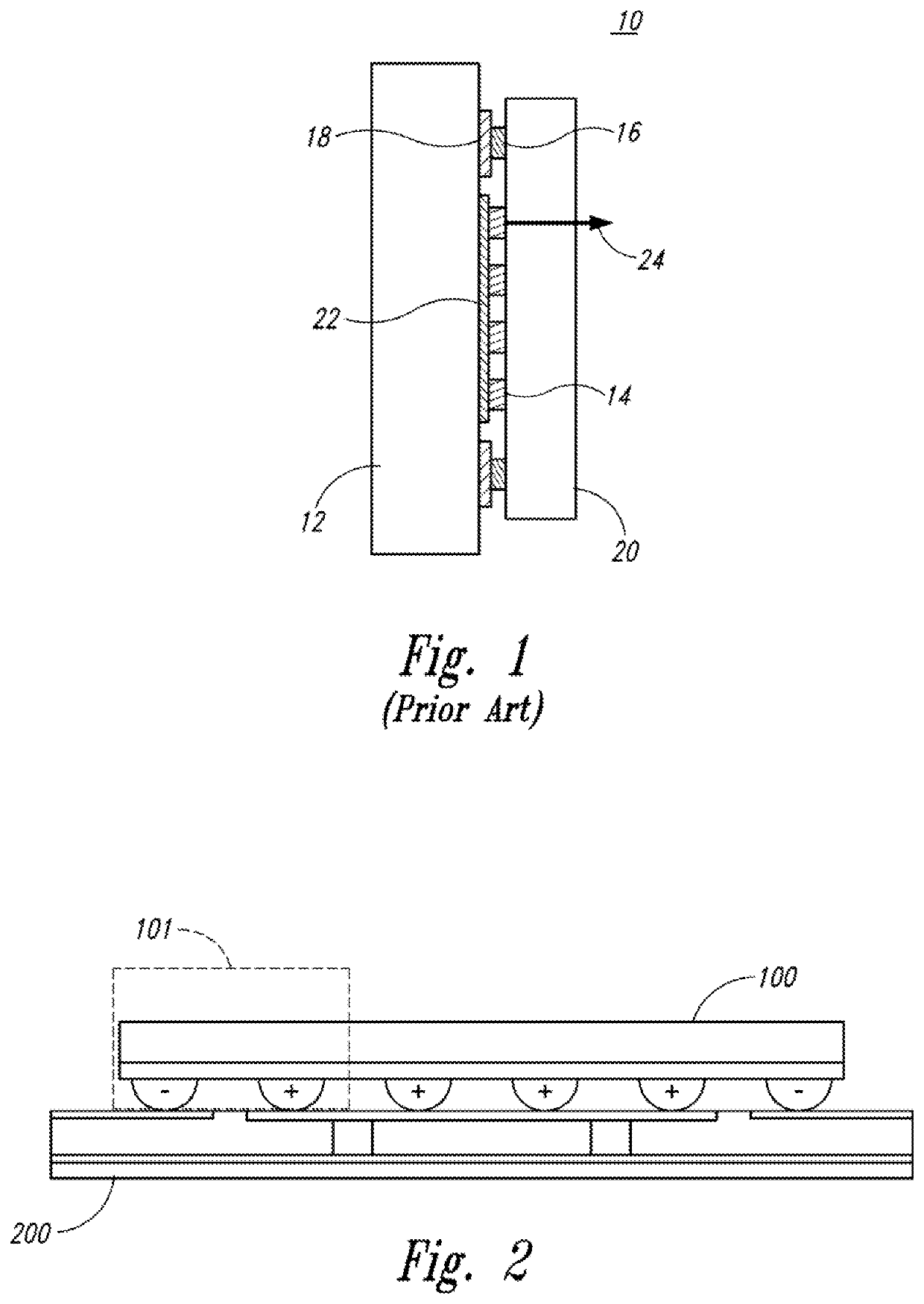
A Surface-Mount Compatible VCSEL Array
a technology of vcsel array and surface mount, which is applied in the direction of semiconductor lasers, laser details, electrical equipment, etc., can solve the problems of not being able to be used directly with high-speed, low-cost surface mount soldering processes commonly used to mass-produce electronic and opto-electronic systems, and the inability to scale wire-bonded devices into two-dimensional arrays. , to achieve the effect of convenient surface mount processing, improved heat removal efficiency
- Summary
- Abstract
- Description
- Claims
- Application Information
AI Technical Summary
Benefits of technology
Problems solved by technology
Method used
Image

Examples
first embodiment
[0072]FIG. 12 illustrates the resulting metal structures a combination of posts 132 and solder metal layer 136 that may provide the actual solder bonding surfaces for the VCSEL array. Copper electroplating of the posts 132 provides a thick structure that can carry large amounts of current with very low loss and low parasitic inductance. The copper posts may be terminated with a metal layer structure optimized for good adhesion and compatibility with common solders used for surface mount assembly. An example is a layer of gold on the surface of the copper posts 132 with a diffusion barrier of nickel followed by a thin corrosion barrier of gold. There are many variations of commonly used under bump metallization (UBM) known to those skilled in the art. The fabrication of the copper posts may require another application of a continuous thin metal seed layer, a thick photoresist layer photolithographically patterned to create the desired size and pitch of copper posts. After electropla...
second embodiment
[0073]A second embodiment is shown in FIG. 13 in which an additional planarization layer 134 of polymer or other dielectric material is applied after the completion of the interposer metal pads 130. This layer can also be patterned and used to define the shapes of the metal posts 132, but may be left in place to insulate the interposer pads from the deposition of the solder 136 and from the soldering reflow process itself. The additional planarization dielectric 134 can also be left higher than the metal posts 132 to facilitate the assembly of discrete solder balls onto the metal post 132 surfaces.
[0074]Another embodiment, shown in FIG. 14, does not use the plated copper posts, but uses a solder wetting barrier 138 directly on the anode and cathode pad metal 130 so that specific areas of the pad can have solder deposited or can be bonded with solder paste applied to the PCB. The solder wetting barriers can be dielectric material or metals known to those skilled in the art to not all...
PUM
| Property | Measurement | Unit |
|---|---|---|
| current spreading loss | aaaaa | aaaaa |
| current | aaaaa | aaaaa |
| thick | aaaaa | aaaaa |
Abstract
Description
Claims
Application Information