
Power semiconductor module

A technology of power semiconductors and conductor rails, applied in the field of power semiconductor modules, which can solve the problems of reduced lifespan, unreliable elimination of cracks, and reduced breakdown strength of power semiconductor modules

Active Publication Date: 2013-08-28
SEMIKRON ELECTRONICS GMBH & CO KG
View PDF1 Cites 0 Cited by
  • Summary
  • Abstract
  • Description
  • Claims
  • Application Information

AI Technical Summary

Problems solved by technology

However, due to the temperature-dependent movability of the substrate with respect to the housing fastened to the cooling structure, cracking of the hardened potting is not reliably eliminated in the known power semiconductor modules, so that inaccuracies occur. The desired air gap with the corresponding permittivity ε for air 0 , and the breakdown strength corresponding to the dielectric constant ε of the hardened perfusion is correspondingly reduced to that of air 0 value of
This means that the lifetime of the power semiconductor modules may be correspondingly reduced

Method used


Image

  • Power semiconductor module
  • Power semiconductor module
  • Power semiconductor module

Examples


Embodiment Construction

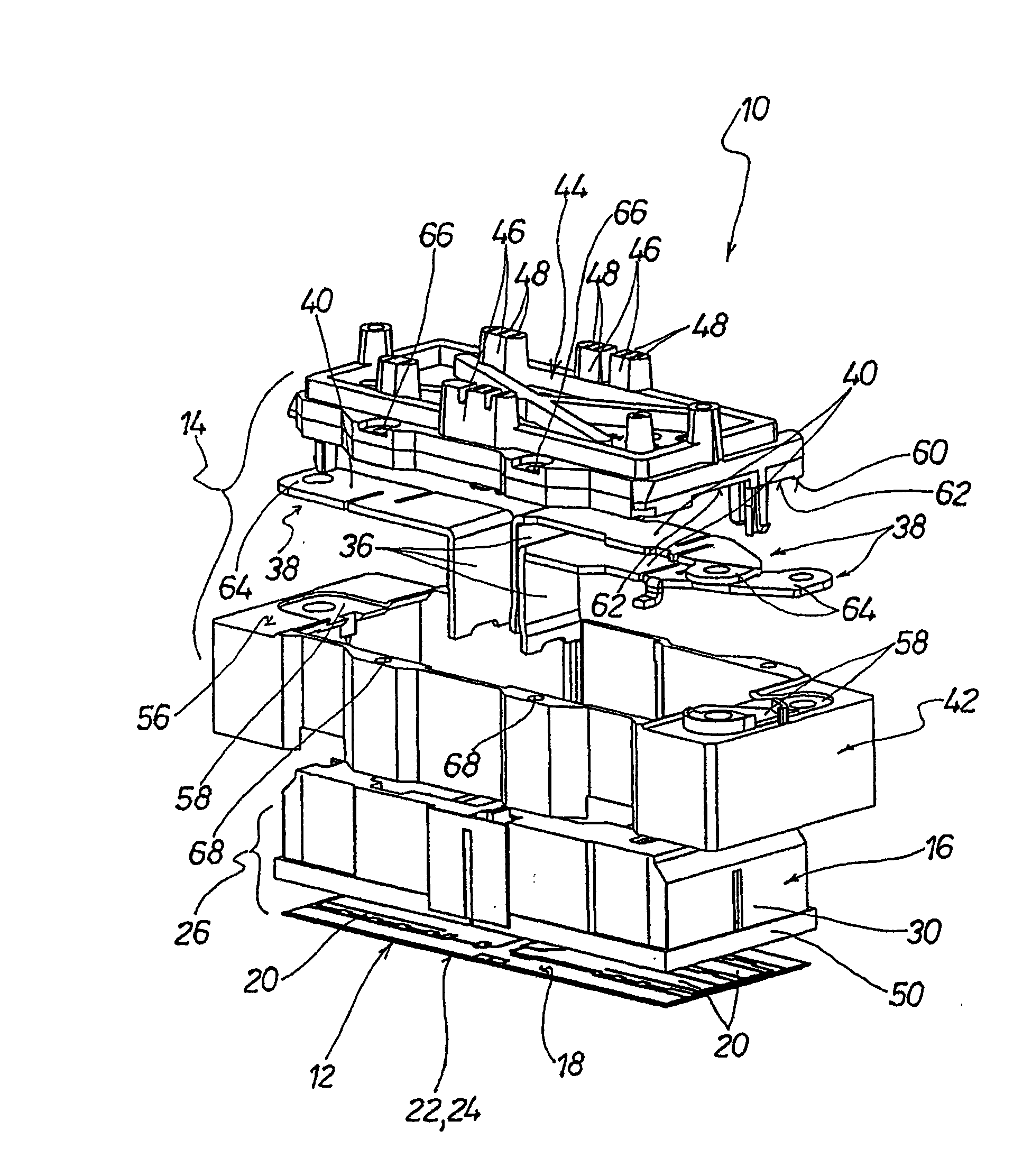
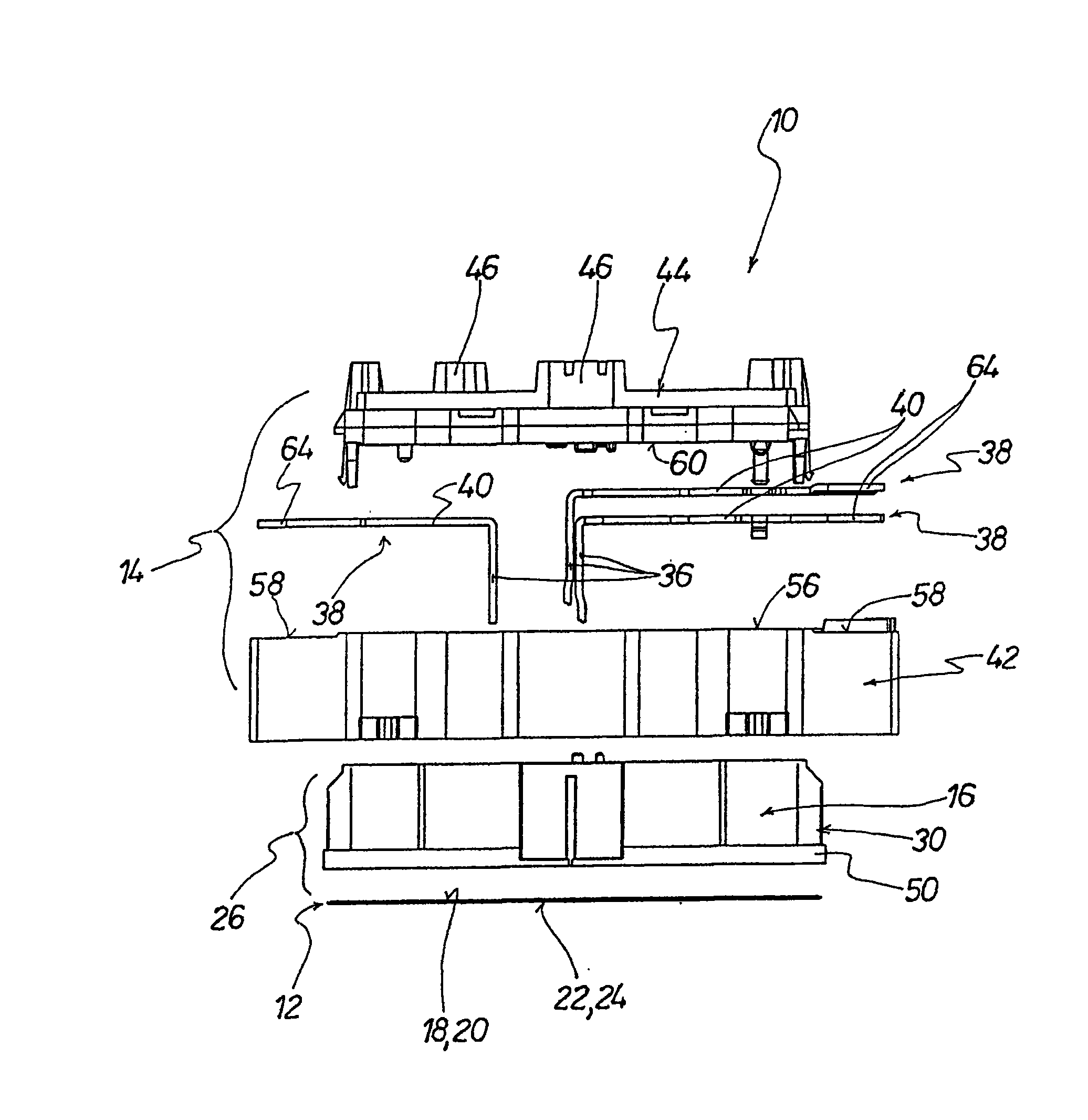
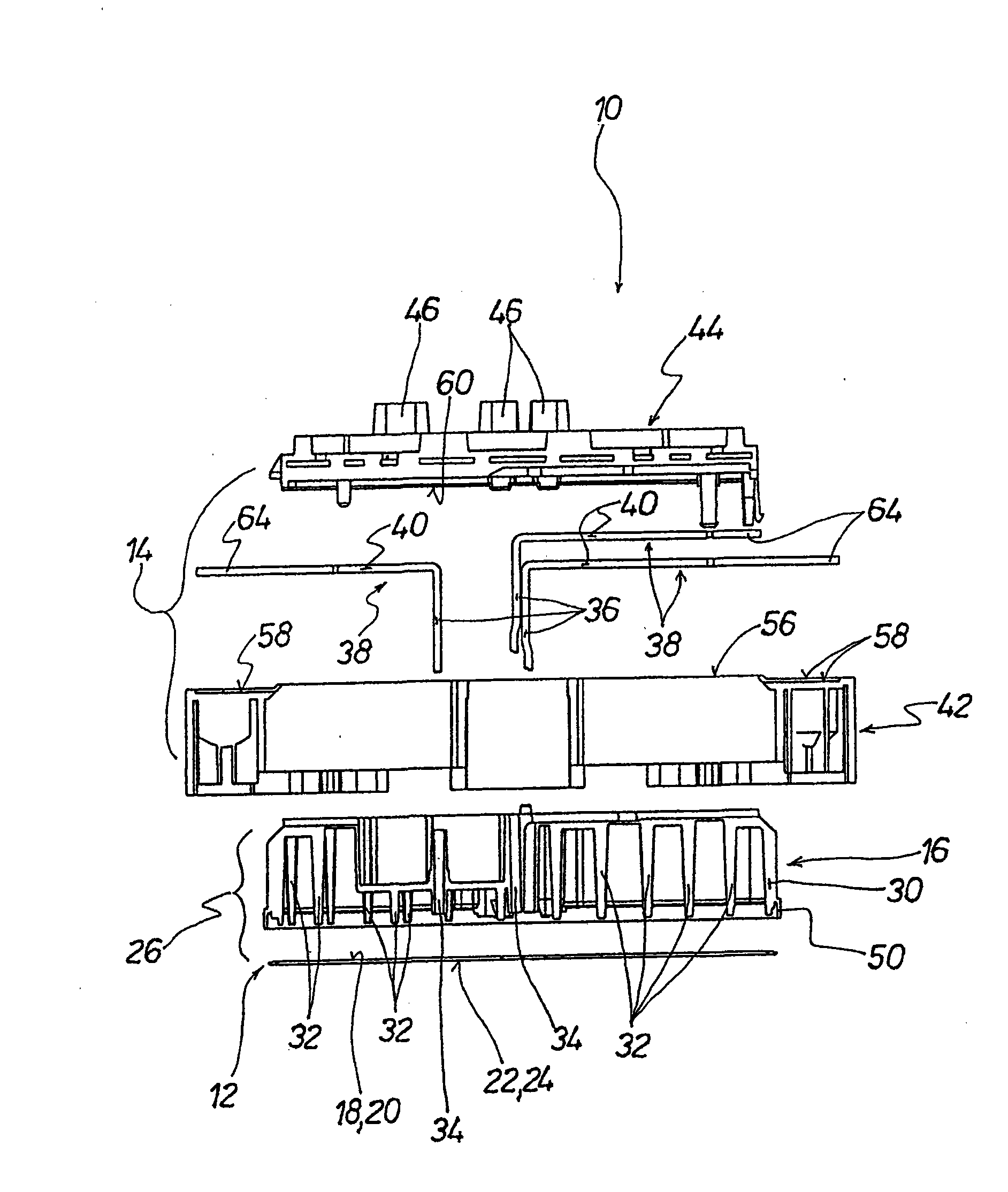
[0018] figure 1 An embodiment of a power semiconductor module 10 is shown, which has a substrate 12 , a housing 14 and a bridge element 16 . as by Figure 4 It can be seen that the substrate 12 has conductor tracks 20 and power semiconductor components (not shown) on the first main surface 18 and a metal layer 24 on the opposite second main surface 22 . A metal layer 24 is provided for dissipating heat to cooling structures (not shown).

[0019] The substrate 12 together with the bridge element 16 forms a structural unit 26 which is movable in a restricted manner in all transverse directions parallel to the first main body surface 18 and the second main body surface 22 in the housing 14 . restricted mobility in Figure 4 is represented by double arrow 28 . Furthermore, movement in a direction perpendicular to said transverse direction is also possible.

[0020] as by image 3 It can be seen that the bridge element 16 is configured in the shape of a cap with an annular si...


PUM


Abstract

The power semiconductor module (10) has a substrate (12), housing (14) and a bridge element (16), where the substrate has a conductive strip (20) for load connection elements (38) and for power semiconductor elements. The conductive strip is provided at a main surface (18), and on opposite to another main surface (22). The substrate forms a component (26) with the bridge element, which is arranged in parallel lateral direction for both main surfaces of the substrate.

Description

technical field [0001] The invention relates to a power semiconductor module having a substrate, a housing and a bridge element, wherein the substrate has elements for load connection and for power semiconductor components on a first body surface and has a metal layer on the opposite second body surface, which is provided for dissipating heat to a cooling structure, wherein the housing can be fastened to the cooling structure, and wherein, The bridge element is arranged on the housing and is arranged in relation to the conductor track of the substrate for positioning the contact section of the load connection element and is pushed against the first main body surface of the substrate by means of the push element. Background technique [0002] Substrate is, for example, a DCB substrate (direct copper bonding). Such power semiconductor modules are required to function reliably over a long period of use in a temperature range of −30° C. to 150° C. Such a large temperature rang...

Claims


Application Information

Patent Timeline
Patent Type & Authority Patents(China)
IPC IPC(8): H01L23/48H01L23/10H01L23/34
CPCH01L2924/16195H01L25/072H01L23/02H01L2924/01079H01L23/48H01L23/34
Inventor 雷纳尔·波浦马库斯·格鲁贝尔
Owner SEMIKRON ELECTRONICS GMBH & CO KG
Learn More