Eureka AIR delivers breakthrough ideas for toughest innovation challenges, trusted by R&D personnel around the world.

Scanning Line Driving Method

A driving method and scanning line technology, applied in the direction of instruments, static indicators, etc., can solve the problems such as the decrease of the aperture ratio of the display, the inability to reach the data voltage level, and the poor display effect.

Inactive Publication Date: 2011-11-30
WINTEK CORP
View PDF0 Cites 0 Cited by
  • Summary
  • Abstract
  • Description
  • Claims
  • Application Information

AI Technical Summary

Problems solved by technology

However, as the resolution of liquid crystal displays increases day by day, the traditional scanning line driving method will shorten the scanning time of each scanning line under the same frame period (Frame Period), so that the voltage on the storage capacitor in the pixel will be charged due to The time is too short to reach the data voltage level to be written, thus causing the problem of poor display effect
However, if the charging speed of the data line is increased by increasing the size of the TFT, the aperture ratio (Aperture Ratio) of the liquid crystal display will be reduced.

Method used


Image

  • Scanning Line Driving Method
  • Scanning Line Driving Method
  • Scanning Line Driving Method

Examples


no. 1 example

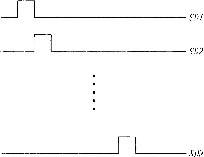
[0028] Please refer to Figure 4 , which shows a waveform diagram of scanning signals according to the scanning line driving method in the first embodiment of the present invention. In this embodiment, two scan signals SD1' and SD2' are taken as an example to illustrate the scan signals driving the odd scan line 310a and the even scan line 310b.

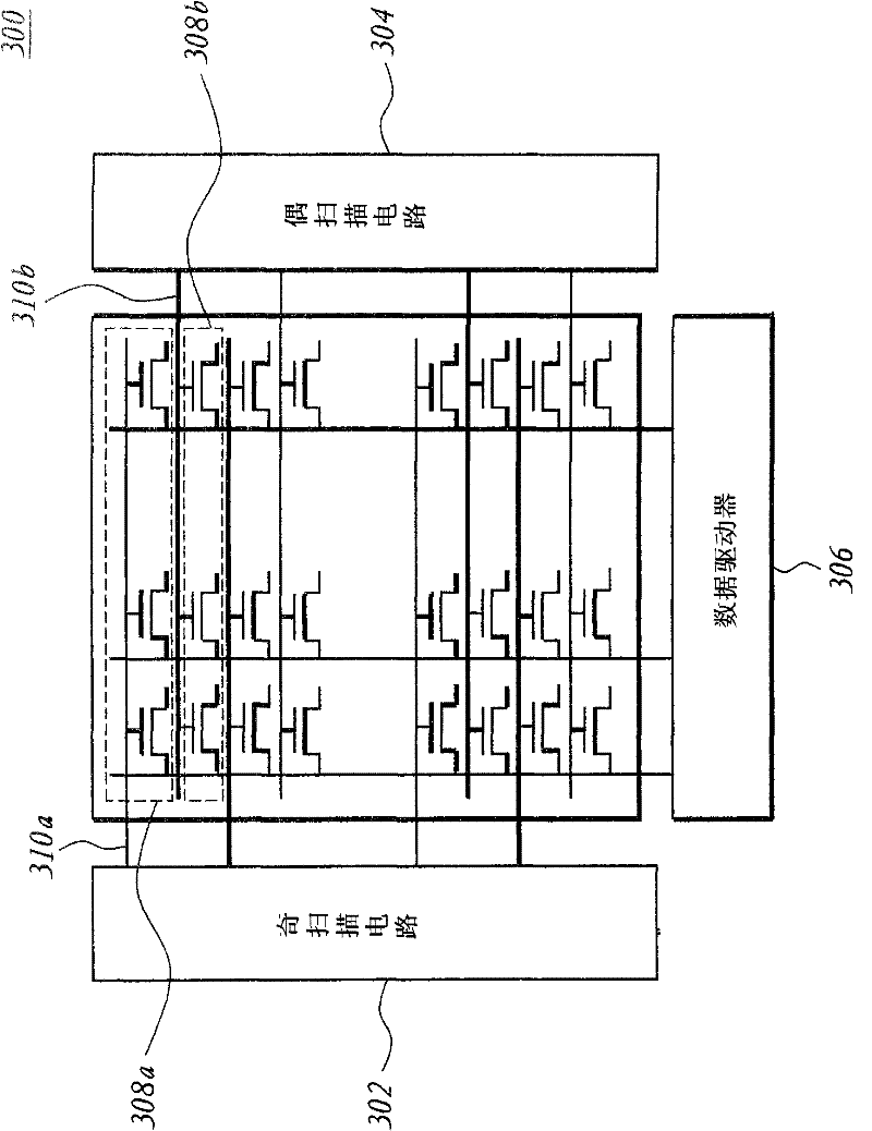
[0029] like Figure 4 As shown, this embodiment is applied to a liquid crystal display 300, and the odd scan circuit 302 and the even scan circuit 304 are used to generate scan signals SD1' and SD2' respectively. The scan signals SD1' and SD2' are used to control the odd-numbered pixel 308a and the even-numbered pixel 308b through the odd scan line 310a and the even scan line 310b, respectively.

[0030] The liquid crystal display 300 includes an odd frame scan period and an even frame scan period due to the polarity inversion of the data voltage. During the scanning period of the odd frame, the pixels 308a in the odd columns and ...

no. 2 example

[0041] Please refer to Figure 7 , which shows a scanning signal waveform diagram according to the scanning line driving method in the second embodiment of the present invention. In this embodiment, the scanning signals SD1 ″ and SD2 ″ are used to represent the scanning signals for driving the odd scanning line 310 a and the even scanning line 310 b respectively, and taking the scanning signals SD1 ″ and SD2 ″ as an example, for the odd scanning line 310 a and the even scanning line 310 a The scanning signal of the scanning line 310b will be described.

[0042] The difference between the second embodiment and the first embodiment is that the scanning signals SD1 ″ and SD2 ″ in the second embodiment have different timing waveforms from the scanning signals SD1 ′ and SD2 ′ in the first embodiment, such as Figure 7 The scanning line driving method of this embodiment shown is to cut the pixel scanning time TS of the odd scanning line 310a and the even scanning line 310b among th...

no. 3 example

[0063] Please refer to Figure 11 , which shows a waveform diagram of scanning signals according to the scanning line driving method in the third embodiment of the present invention. The scanning line driving method of the third embodiment is applied to the liquid crystal display 300 . In this embodiment, the N columns of pixels 308 of the LCD 300 are controlled by cutting the pixel scanning time TS of the N scanning lines 310 in the LCD 300 to achieve the effects of pre-charging and pre-discharging. This embodiment takes four scan lines as an example to illustrate the operation method of N scan lines 310 in the liquid crystal display 300 .

[0064] The scan signals SD1 ″’ and SD3 ″’ are generated by the odd scan circuit 302 , and the scan signals SD2 ″’ and SD4 ″’ are generated by the even scan circuit 304 . The scan signals SD1"' and SD3"' are used to respectively control the first and third columns of pixels in the odd columns of pixels 308a through the first scan line an...


PUM


Abstract

A scanning line driving method of a display is to cut the scanning time of a first scanning line (ScanLine) and a second scanning line in a liquid crystal display, so that the enabling time of the first scanning line and the second scanning line are respectively equal to a charging time and a discharging time. Wherein the first scan line and the second scan line are respectively used to control a first row of pixels and a second row of pixels of the liquid crystal display.

Description

[0001] This application is a divisional application of the invention patent application with the application number 200610141628.9 and the invention name "Drive Method of Scanning Line" submitted by the applicant on September 28, 2006. technical field [0002] The present invention relates to a scanning line driving method, and in particular to a scanning line driving method of a liquid crystal display. Background technique [0003] Please refer to figure 1 , which shows a circuit block diagram of a conventional liquid crystal display. The liquid crystal display 100 includes a data driving circuit 102 , a scanning driving circuit 104 , N columns of pixels 106 , a plurality of data lines 108 and N scanning lines 110 , where N is a natural number greater than 1. [0004] The scan driving circuit 104 is used to output N scan signals through N scan lines to respectively drive N columns of pixels 106 . The data line driving circuit 102 is used for outputting pixel data through ...

Claims


Application Information

Patent Timeline
Patent Type & Authority Patents(China)
IPC IPC(8): G09G3/36G09G3/20G02F1/133
Inventor 林林梁宝芝黄俊铭赖志章陈泰源蒋圣评
Owner WINTEK CORP
Why Eureka
Eureka Blog
Learn More