Probe testing device

A test device and probe technology, applied in the direction of measurement device, measurement of electricity, measurement of electrical variables, etc., can solve problems such as height restrictions

Active Publication Date: 2010-02-10
MICROELECTRONICS TECH INC
View PDF2 Cites 13 Cited by
  • Summary
  • Abstract
  • Description
  • Claims
  • Application Information

AI Technical Summary

Problems solved by technology

[0008] The main purpose of the present invention is to provide a probe testing device, which is easy to manuf

Method used


Image

  • Probe testing device
  • Probe testing device
  • Probe testing device

Examples


Embodiment Construction

[0033] In order to describe the structure, features and functions of the present invention in detail, the following preferred embodiments are given and described with reference to the drawings.

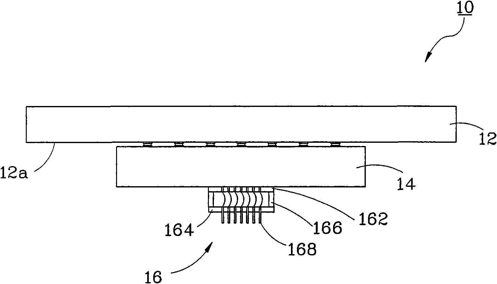
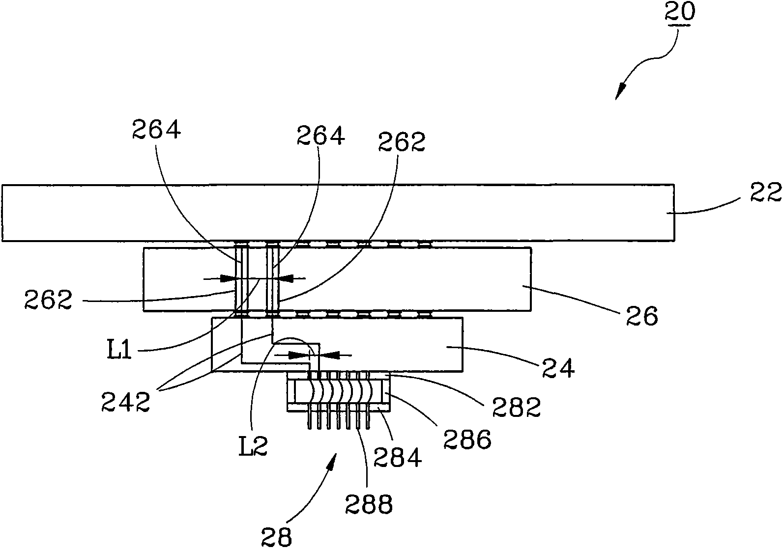
[0034] see image 3 , the probe testing device 20 provided by the first preferred embodiment of the present invention includes a circuit board 22 , a space transformer board 24 , a riser board 26 and a vertical probe set 28 .

[0035] In this embodiment, the space transformer 24 is a multi-layer organic structure (Multi-Layered Organic, MLO) with a plurality of circuits 242 inside.

[0036] In this embodiment, the riser plate 26 is a multi-layer ceramic structure (Multi-Layered Ceramic, MLC), which has higher heat resistance than the space transformer plate 24 . The riser board 26 is electrically connected to the space transformer board 24 through the first reflow, and then electrically connected to the circuit board 22 through the second reflow. The riser board 26 has a plurality o...


PUM


Abstract

The invention provides a probe testing device, which is mainly characterized in that: a booster board is arranged between a circuit board and a space converter board and a plurality of probes are arranged on the space converter board, so that the fixed height between the surface of the circuit board and the tips of the probes can be overcome through the booster board, a space converter board withlarge thickness is not needed to be manufactured, and the difficulty and cost of manufacturing the probe testing device can be effectively reduced.

Description

technical field [0001] The invention relates to a probe testing device, in particular to a probe testing device which can effectively reduce manufacturing difficulty and cost. Background technique [0002] see figure 1 The shown conventional vertical probe card 10 mainly includes a circuit board 12, a space transformer 14 disposed on the lower surface 12a of the circuit board 12, and a vertical probe group 16 disposed on the space transformer 14, Wherein the vertical probe set 16 has an upper guide plate 162 and a lower guide plate 164 arranged on the space conversion plate 14, a spacer 166 respectively connected to the upper and lower guide plates 162 and 164, and a plurality of upper and lower guide plates 162 pierced through, 164 vertical probes 168. [0003] Since the height from the lower surface 12b of the circuit board 12 to the needle points of these vertical probes 168 is often limited by the use environment of the testing machine, the height of the upper and ...

Claims


Application Information

Patent Timeline
IPC IPC(8): G01R1/067G01R1/073
Inventor 孙宏川简志忠杨惠彬吴坚州黄朝敬施伯宗
Owner MICROELECTRONICS TECH INC
Why Eureka
Try Eureka