
Eureka
For R&D, Eureka makes reading and utilizing patents & technical documents easy.
Eureka AIR
Designed for self-driven R&D workflows. Generate viable solutions, solve complex R&D challenges, empower your innovation with AI.

Eureka Materials
Designed for material experts only. Revolutionize your material R&D, from search, analyze, to developing new materials.

TechResearch
Generate reliable direction feasibility study reports for your R&D in just a few steps.

TechSeek
Discover and master advanced knowledge NOW. Basics, ideas, possibilities, all at once.

TechMind
As an expert in R&D Theories, TechMind can generates customized viable solutions instantly.

TechRisk
Analyze your overall solution with one click, know your potential R&D risks in advance.

TechMonitor
Get weekly tech updates, stay abreast of the latest tech innovations and key insights.
Exposure device, light-emitting device, image forming apparatus and failure diagnosing method
A technology of exposure device and light-emitting element, which is applied to the electrical recording process using the charge pattern, equipment and optics of the electric recording process using the charge pattern, and can solve problems such as light-emitting failures and image loss, and achieve reliable transfer of failures and simplify structure effect
- Summary
- Abstract
- Description
- Claims
- Application Information
AI Technical Summary
Problems solved by technology
Method used
Image

Examples
Embodiment Construction
[0038] Hereinafter, exemplary embodiments of the present invention will be described in detail with reference to the accompanying drawings.
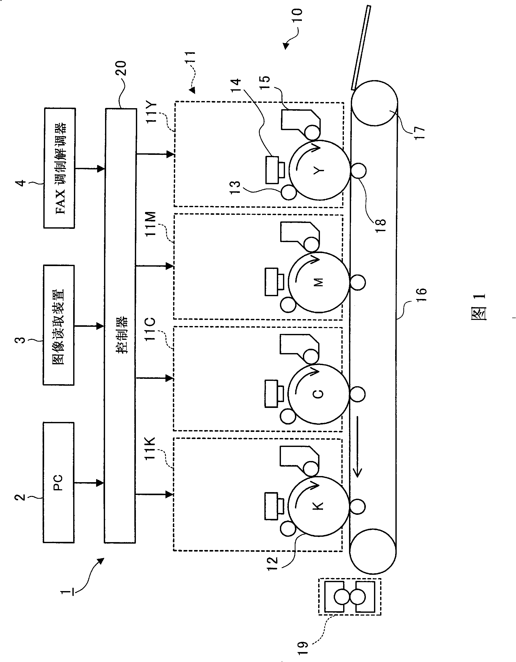
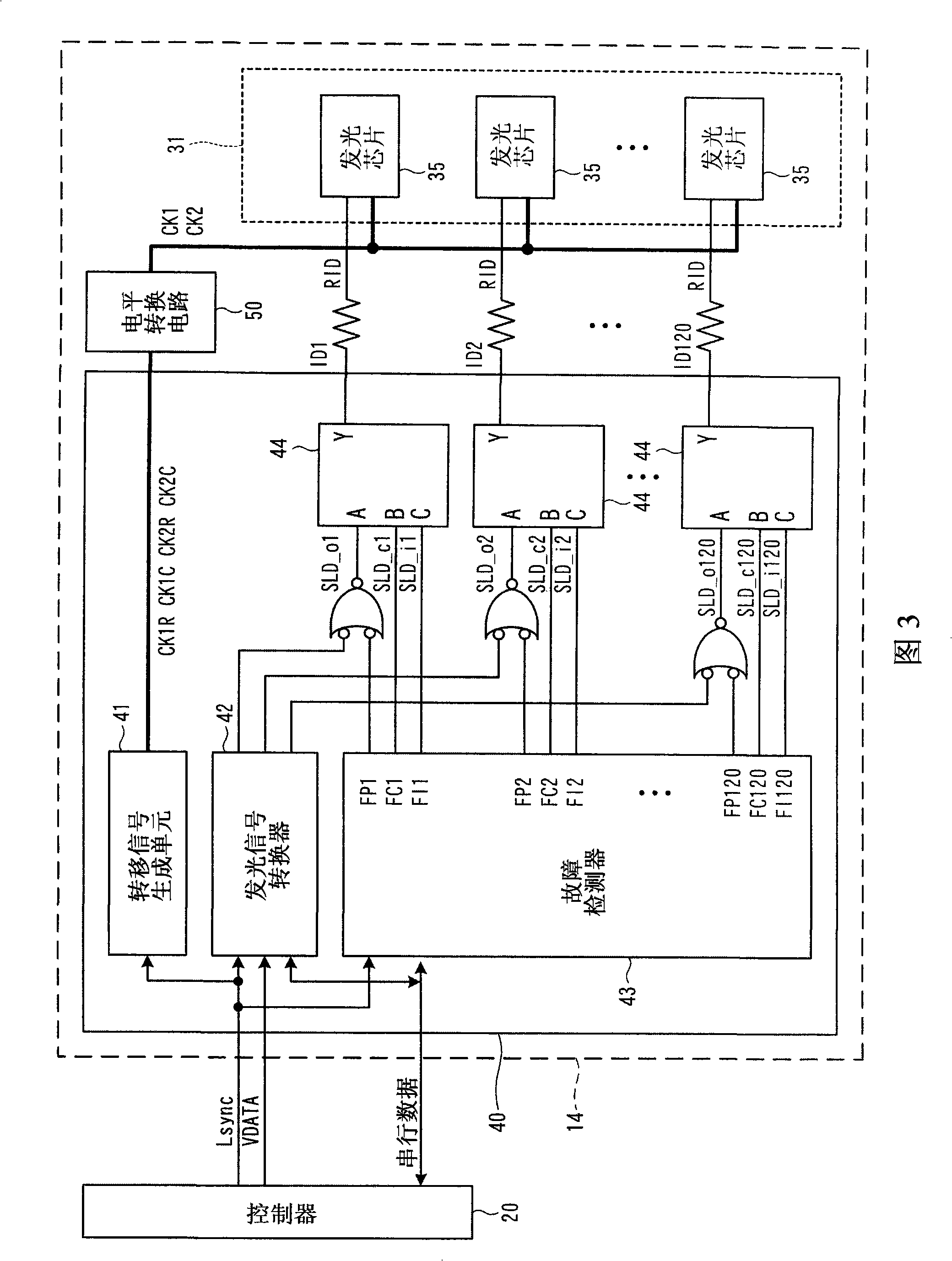
[0039] figure 1 An overall configuration example of an image forming apparatus 1 to which the exemplary embodiment is applied is shown. The image forming apparatus 1 includes an image forming processing unit 10 and a controller 20 . The image formation processing unit 10 forms images respectively corresponding to image data sets of different colors. A controller 20 connected to an external device such as a personal computer (PC) 2, or an image reading device 3 or a FAX (facsimile machine) modem 4 performs image processing on image data received from the above devices, and controls the entire image forming device 1 operation.
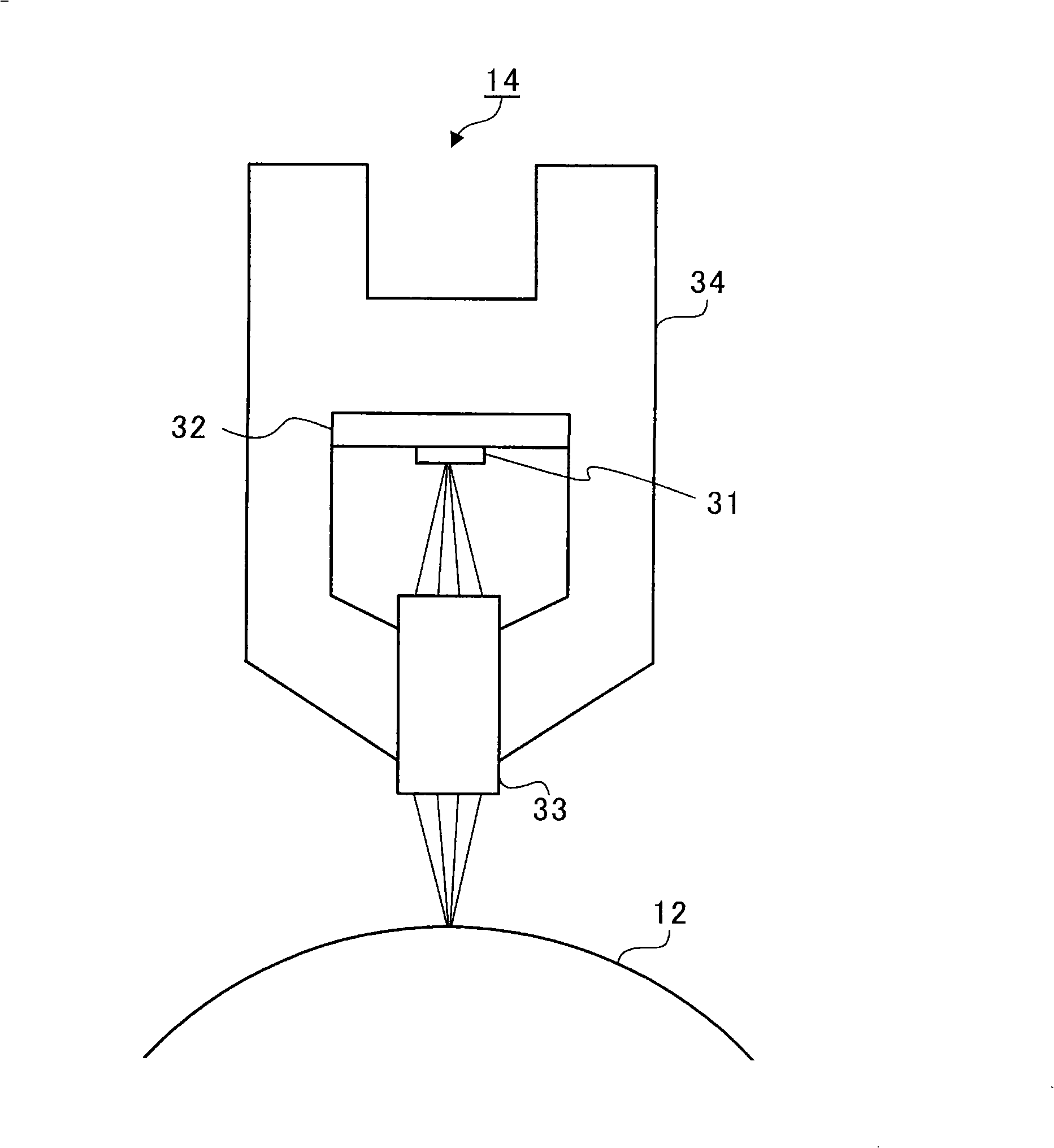
[0040] The image forming processing unit 10 includes four image forming units 11 (specifically, 11Y, 11M, 11C, and 11K) arranged at regular intervals. Each image forming unit 11 includes a photosensitive drum 1...
PUM
 Abstract
Description
Claims
Application Information
 - R&D Engineer
- R&D Manager
- IP Professional
- Industry Leading Data Capabilities
- Powerful AI technology
- Patent DNA Extraction
Browse by: Latest US Patents, China's latest patents, Technical Efficacy Thesaurus, Application Domain, Technology Topic, Popular Technical Reports.
© 2024 PatSnap. All rights reserved.Legal|Privacy policy|Modern Slavery Act Transparency Statement|Sitemap|About US| Contact US: help@patsnap.com