Automatic detection system and detection method of high resolution printed circuit board

A printed circuit board, automatic detection technology, applied in measurement devices, analysis materials, material analysis using radiation, etc., can solve the problems of inability to test, high cost, limited test coverage, achieve accurate defect identification, reduce Clarity, hardware for simple effects

Inactive Publication Date: 2010-05-12
ZHONGBEI UNIV
View PDF0 Cites 53 Cited by
  • Summary
  • Abstract
  • Description
  • Claims
  • Application Information

AI Technical Summary

Problems solved by technology

The bed of needle tester also has many disadvantages: different templates need to be made for different circuit boards, the production and debugging cycle is long, and the cost is high, so it is not suitable for the test of low-volume prototypes; the test coverage is limited. Only short circuit and open circuit can be tested Defects, shielded assemblies cannot be tested; as board density becomes higher and

Method used


Image

  • Automatic detection system and detection method of high resolution printed circuit board
  • Automatic detection system and detection method of high resolution printed circuit board
  • Automatic detection system and detection method of high resolution printed circuit board

Examples


Embodiment Construction

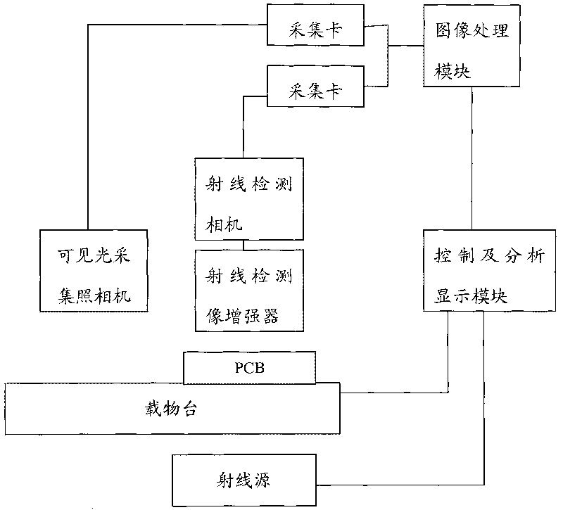
[0032] Such as figure 1 As shown, the detection system is composed of a ray source, a stage, a visible light collection camera, a ray detection camera, a ray detection image intensifier and an acquisition card, an image processing module, and a control and analysis display module. The sources are respectively connected to the control and analysis display modules through connecting lines. The stage is set with two initial positions, which are respectively the visible light shooting position and the radiation detection position. The position is provided with a radiation detection camera and a radiation detection image intensifier, and the radiation detection camera takes images in the radiation detection image intensifier; the visible light acquisition camera and the radiation detection camera are respectively connected through an acquisition card and an image processing module, and the image The processing module is connected to the control and analysis display module through the...


PUM


Abstract

The invention discloses an automatic detection system and method of a high resolution printed circuit board. The detection system comprises a ray source, an object stage, a visible light collection camera, a ray detecting camera, a ray detecting image intensifier, a collection card, an image processing module and a control and analysis display module, wherein the object stage and the ray source are respectively connected with the control and analysis display module through a connecting line, the visible light collection camera and the ray detecting camera are respectively connected with the image processing module through the collection card, and the image processing module is connected with the control and analysis display module through a connecting circuit. The invention combines functions of visible light image navigation, X-ray detection, automatic analysis test marking and the like, is a detection for making quantification aiming to the quality of welding spots and tracing lines and realizes defect automatic detection of invisible welding spots and internal tracing lines.

Description

technical field [0001] The invention relates to a high-resolution printed circuit board automatic detection system and detection method. Background technique [0002] The techniques used for printed circuit board inspection are mainly divided into two categories: electrical testing methods and visual testing methods. Electrical testing usually uses a Wheat bridge to measure the impedance characteristics between network points to detect all continuity. Vision testing finds defects by visually inspecting features of electronic components as well as features of printed wiring. [0003] Currently commonly used detection methods for printed circuit board detection are: [0004] 1. Online testing (ICT, In Circuit Testing) [0005] Check the electrical performance of the online components on the finished board and the connection of the circuit network. It can quantitatively measure resistance, capacitance, inductance, crystal oscillator and other devices, perform functional tes...

Claims


Application Information

Patent Timeline
IPC IPC(8): G01N21/956G01N23/04G01N23/18
Inventor 王明泉曲肇文侯慧玲王玉
Owner ZHONGBEI UNIV
Why Eureka
Try Eureka