Method for constructing and simulating MOSFET mismatch model

A mismatch model and simulation method technology, applied in special data processing applications, instruments, electrical digital data processing, etc., can solve the problem of not specifically describing the error situation, and achieve the effect of improving work efficiency

Active Publication Date: 2010-06-16
SHANGHAI HUAHONG GRACE SEMICON MFG CORP
View PDF0 Cites 18 Cited by
  • Summary
  • Abstract
  • Description
  • Claims
  • Application Information

AI Technical Summary

Problems solved by technology

However, the existing device models usually do not specifically describe the actual e

Method used


Image

  • Method for constructing and simulating MOSFET mismatch model
  • Method for constructing and simulating MOSFET mismatch model
  • Method for constructing and simulating MOSFET mismatch model

Examples


Embodiment Construction

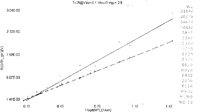
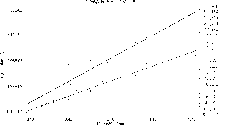
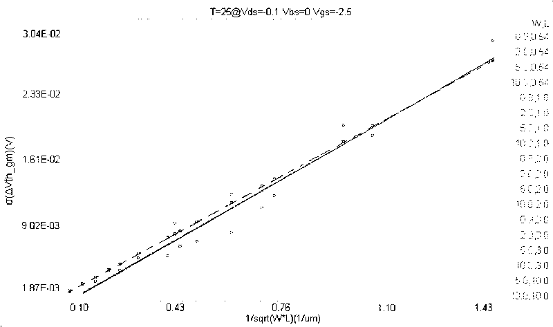
[0034] Such as Figure 5 As shown, the establishment and simulation method of the MOSFET mismatch model of the present invention are divided into the following steps:

[0035] 1. Using statistical principles to establish statistical expressions for random errors in model parameters;

[0036] It is assumed that a device parameter P is a function determined by process parameters such as q1, q2, . . . , qn, ie: P=f(q1, q2, q3, . If there is a slight difference in each process parameter between two identical devices, the expression for the error σ of the parameter P is:

[0037] σ ΔP 2 = ( ∂ f ∂ q 1 ) 2 σ Δq 1 2 ...


PUM


Abstract

The invention discloses a method for constructing and simulating an MOSFET mismatch model, which adopts a BSIM3 model as a basis and is divided into the following steps of: (1) constructing a model parameter random error statistics expression by the principle of statistics; (2) according to the physical definition of the model parameter random error statistics expression, selecting model parameters with pertinence in the BSIM3 model respectively and adding a statistics expression correction term to the model parameters; (3) constructing a corresponding SPICE macro model; (4) defining the initial value of a correction coefficient; (5) substituting the initial value of the correction coefficient into the model and debugging and simulating the model parameters. By regulating the coefficient of a mismatch error function correction formula in the model, the invention can enable the model to accurately describe the trend of the mismatch error of an actual process. By debugging the parameters, the monitoring trend line of the actual process and the simulation trend line of the model can greatly approach to each other. The modeling method can conveniently and better simulate the mismatch statistical error of the actual process.

Description

technical field [0001] The invention relates to a modeling method of a semiconductor device, in particular to a method for establishing and simulating a MOSFET mismatch model. Background technique [0002] In the process of circuit design, the existence of device process mismatch error will cause a certain deviation in the design. In general, factors such as differences in gate oxide thickness, device size, and spacing between devices will have an impact on the process mismatch error. [0003] Therefore, with the improvement of circuit design requirements, the requirement for model accuracy is not only reflected in the electrical characteristics, but also needs to be able to reflect the characteristic error caused by the mismatch of the process. However, the existing device models usually do not specifically describe the actual error situation except for describing the upper and lower limits of the process level. Therefore, it is necessary to establish the description func...

Claims


Application Information

Patent Timeline
IPC IPC(8): G06F17/50
Inventor 王正楠周天舒
Owner SHANGHAI HUAHONG GRACE SEMICON MFG CORP
Why Eureka
Try Eureka