
Dicing die-bonding film and process for producing semiconductor device

A bonding film and cutting film technology, which is applied in semiconductor devices, semiconductor/solid-state device manufacturing, electric solid-state devices, etc., can solve the problems of large semiconductor chips, difficult to pick up semiconductor chips, and difficult to prepare cutting die-bonding films, etc. Achieves the effect of improving low pollution and excellent balance characteristics

Inactive Publication Date: 2010-06-16
NITTO DENKO CORP
View PDF3 Cites 22 Cited by
  • Summary
  • Abstract
  • Description
  • Claims
  • Application Information

AI Technical Summary

Problems solved by technology

[0006] However, even with this improved method, it is sometimes difficult to produce a dicing die-bonding film that well balances the holding force at the time of dicing and the subsequent required peelability.
For example, in the case of obtaining a large semiconductor chip having a size of 10 mm x 10 mm or more, it is not easy to pick up the semiconductor chip by a conventional die bonder because the semiconductor chip size is too large

Method used


Image

  • Dicing die-bonding film and process for producing semiconductor device
  • Dicing die-bonding film and process for producing semiconductor device
  • Dicing die-bonding film and process for producing semiconductor device

Examples


Embodiment 1

[0177]

[0178] Acrylic polymer X was obtained by mixing 95 parts of 2-ethylhexyl acrylate (hereinafter referred to as "2EHA" in some cases), 5 parts of 2-hydroxyethyl acrylate (hereinafter referred to as "HEA" in some cases), ”) and 65 parts of toluene were charged into a reactor equipped with a cooling pipe, a nitrogen gas introduction pipe, a thermometer and a stirring device, followed by polymerization treatment at 61° C. for 6 hours in a nitrogen stream.

[0179] Acrylic polymer Y was obtained by adding 24.1 parts of 2-methacryloxyethyl isocyanate (referred to as "MOI" in some cases) (90 mol % based on HEA) to 100 parts of acrylic polymer X , followed by an addition reaction at 50°C for 48 hours in an air stream.

[0180] Next, a pressure-sensitive adhesive solution of an active energy ray-curable pressure-sensitive adhesive was prepared by mixing 3 parts of a polyisocyanate compound (trade name "COLONATEL", manufactured by Nippon Polyurethane Industry Co., Ltd.), 35 pa...

Embodiment 2

[0186]

[0187]Based on 100 parts of acrylate-based polymer having ethyl acrylate-methyl methacrylate as the main component (trade name "PARACRONW-197CM", produced by Negami Chemical Industrial Co., Ltd.), 102 parts of epoxy resin 1 (trade name "EPICOAT 1004", produced by Japan Epoxy Resins (JER) Co., Ltd.), 13 parts of epoxy resin 2 (trade name "EPICOAT 827", produced by Japan Epoxy Resins (JER) Co., Ltd. ), 119 parts of phenolic resin (trade name "MILEXXLC-4L", produced by Mitsui Chemicals, Inc.), 222 parts of spherical silica (trade name "SO-25R", produced by Admatechs Co., Ltd.) were dissolved in methyl ethyl ketone, thereby preparing a binder composition solution having a solid concentration of 23.6% by weight.

[0188] The adhesive composition solution was applied on a release-treated film consisting of a PET film having a thickness of 38 μm on which silicone release treatment had been performed as a release liner (separator), and then at 130 °C for 2 minutes. Thus, ...

Embodiment 3 to 7

[0191] A dicing die-bonding film was produced in each of Examples 3 to 7 in the same manner as in Example 1 except that the dicing film was changed to the corresponding dicing film having the composition and content shown in Table 1.


PUM

PropertyMeasurementUnit
thicknessaaaaaaaaaa
particle sizeaaaaaaaaaa
thicknessaaaaaaaaaa

Abstract

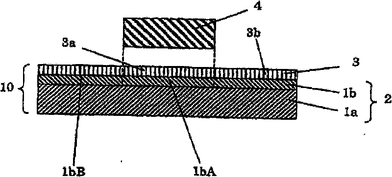
The present invention relates to a dicing die-bonding film comprising: a dicing film having a pressure-sensitive adhesive layer provided on a base material; and a die-bonding film provided on the pressure-sensitive adhesive layer, in which the pressure-sensitive adhesive layer of the dicing film is an active energy ray-curable heat-expandable pressure-sensitive adhesive layer containing a foaming agent, and in which the die-bonding film is constituted by a resin composition containing an epoxy resin. Moreover, the present invention provides a process for producing a semiconductor device which includes using the above-described dicing die-bonding film.

Description

technical field [0001] The present invention relates to a dicing die-bonding film for dicing a chip-shaped workpiece such as a semiconductor chip by disposing an adhesive for fixing an electrode member on the workpiece such as a semiconductor wafer before dicing. Background technique [0002] After the thickness thereof is adjusted by back grinding as necessary, the semiconductor wafer (work) on which the circuit pattern is formed is diced into semiconductor chips (chip-shaped work) (dicing step). During the dicing step, semiconductor wafers are usually applied with moderate hydraulic pressure (typically, about 2 kg / cm 2 ) to remove the cut layer. Then, the semiconductor chip is fixed on an adherend such as a lead frame with an adhesive (mounting step), and then shifts to a bonding step. Adhesives are already applied to lead frames or semiconductor chips during conventional mounting steps. However, in this method, it is difficult to make the adhesive layer uniform, and sp...

Claims


Application Information

Patent Timeline
Patent Type & Authority Applications(China)
IPC IPC(8): H01L21/00H01L21/68H01L21/304B28D5/00C09J133/08B32B7/12
CPCH01L2924/01051H01L2924/07802H01L2924/01027H01L24/83H01L24/85H01L24/29H01L2224/73265H01L2924/01016H01L2224/27436H01L2924/01045H01L2224/32225H01L2924/01015B32B7/12H01L2221/68318H01L2924/01047H01L2224/8385H01L21/6835H01L2224/48091H01L2924/01006H01L2924/01079H01L2924/01074H01L2924/10253H01L2924/01041H01L2924/01024H01L2924/01005H01L2924/01082H01L2224/85H01L2224/2919H01L2924/01013H01L2924/19042H01L2924/01056H01L2221/68327H01L2924/01011H01L2224/92247H01L2924/014H01L2224/83191B32B27/38H01L2924/01029H01L21/6836H01L24/27H01L2224/48227H01L2224/92H01L2924/01033H01L2924/0665H01L2924/0102H01L2924/01075B32B3/08B32B5/18B32B15/04B32B23/04B32B25/12B32B25/14B32B27/08B32B27/18B32B27/20B32B27/22B32B27/281B32B27/285B32B27/286B32B27/30B32B27/32B32B27/34B32B27/36B32B27/365B32B27/40B32B29/002B32B2255/205B32B2307/21B32B2307/306B32B2307/3065B32B2307/516B32B2307/518B32B2307/54B32B2457/14H01L24/48H01L24/73H01L2924/00014H01L2924/15747H01L2924/15788H01L2924/181Y10T428/249971Y10T428/249984H01L2924/00H01L2924/00012H01L2924/3512H01L2224/45015H01L2924/207H01L2224/45099
Inventor 神谷克彦大竹宏尚松村健村田修平
Owner NITTO DENKO CORP
Learn More