Printed circuit board shielding method and printed circuit board

A technology for printed circuit boards and shielding layers, which is applied to printed circuits, printed circuits, printed circuit components, etc., can solve the problems of high shielding cost and long production cycle, and achieve the effects of simplifying production, reducing costs, and ensuring shielding effects

Active Publication Date: 2010-06-16
HUAWEI DEVICE CO LTD
View PDF0 Cites 17 Cited by
  • Summary
  • Abstract
  • Description
  • Claims
  • Application Information

AI Technical Summary

Problems solved by technology

[0005] Embodiments of the present invention provide a printed circuit board shielding method and a printed circuit board to overcome the defects of high shielding cost and long production cycle of existing printed circuit boards

Method used


Image

  • Printed circuit board shielding method and printed circuit board
  • Printed circuit board shielding method and printed circuit board
  • Printed circuit board shielding method and printed circuit board

Examples


Embodiment 1

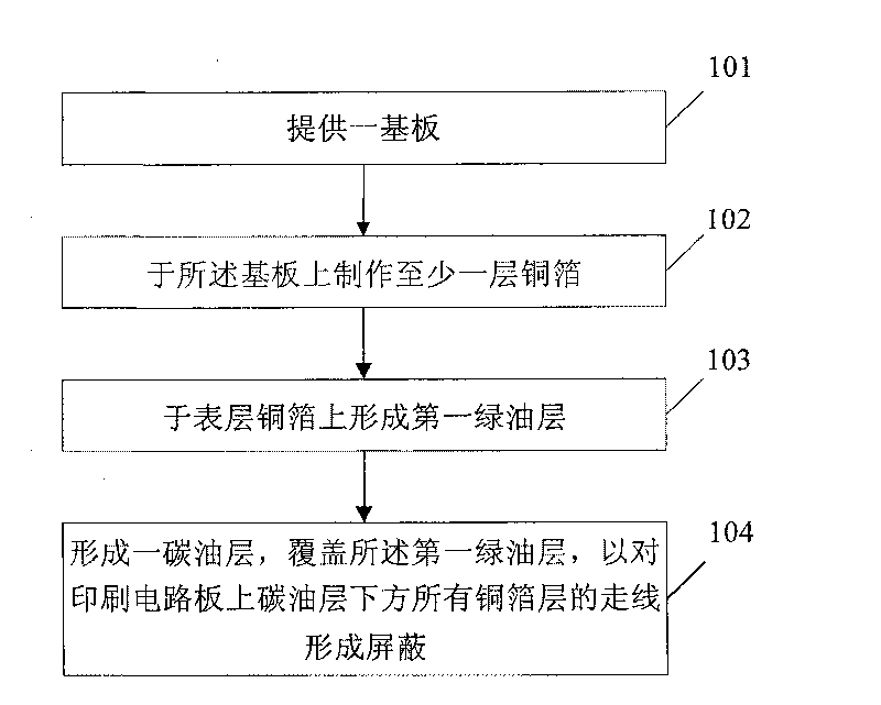
[0015] This embodiment provides a method for shielding a printed circuit board. like figure 1 As shown, the method includes:

[0016] Step 101: providing a substrate;

[0017] Step 102: making at least one layer of copper foil on the substrate;

[0018] In this step, copper foil is fabricated on the surface of the substrate, and the number of layers of copper foil can be 2, 4, 6, etc. multi-layer.

[0019] Step 103: forming a first green oil layer on the surface copper foil;

[0020] In the case of making multi-layer copper foil, the first green oil layer is formed only on the outermost copper foil, that is, the surface copper foil.

[0021] The above three steps can be done using the current commonly used process. The green oil layer covers the surface copper foil, and the position that needs to be connected to the electronic components is exposed. In addition, according to actual process requirements, the positions where the surface copper foil needs to be grounded can ...

Embodiment 2

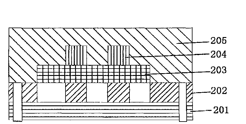
[0034] This embodiment provides a printed circuit board, which is made by the method described in Embodiment 1, such as figure 2 As shown, the printed circuit board includes:

[0035] A substrate 201;

[0036] At least one layer of copper foil 202 is fabricated on the substrate;

[0037] The first green oil layer 203 is formed on the surface copper foil 202;

[0038] In this embodiment, only one layer of copper foil is taken as an example, but it is not limited thereto. In practical applications, circuit boards with different layers of copper foil such as 2, 4, 6, and 8 can be made according to needs, but the first green oil layer And the subsequent insulating layer and carbon oil layer are only formed on the outermost surface copper foil.

[0039] The three-layer structure of the above printed circuit board is the same as that of the prior art printed circuit board.

[0040] A carbon oil layer 205 covers the first green oil layer 203 to form a shield for all copper foil ...

Embodiment 3

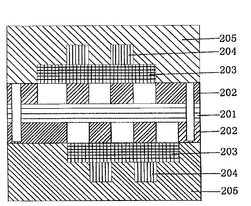
[0048] This embodiment provides a printed circuit board, which is made by the method described in Embodiment 1, such as image 3 As shown, compared with the second embodiment, the printed circuit board provided by this embodiment is double-sided. Double-sided wiring shielding is an expansion on the basis of Embodiment 2. It is outside the double-sided strong radiation wiring of the PCB, each covered with a layer of carbon film and grounded for shielding. The structure of each layer is the same as that of Embodiment 2. No longer.


PUM


Abstract

The invention provides a printed circuit board shielding method and a printed circuit board. The method comprises the steps of providing a substrate, manufacturing at least one layer of copper foil on the substrate; forming a first green oil layer on surface-layer copper coil; and forming a carbon oil layer to cover the green oil layer so as to shield the routing of all copper coil layers arranged under the carbon oil layer on the printed circuit board. The printed circuit board comprises the substrate, at least one layer of copper foil manufactured on the substrate, the first green oil layer formed on the surface-layer copper coil, and the carbon oil layer covered on the first green oil layer. Aiming at the disadvantages of increased cost caused by adding copper coils and shielding layers to shield in the printed circuit board in the prior art, in the embodiment of the invention, routing of printed circuit boards are shielded by carbon films, thereby ensuring shielding effect, lowering cost and simplifying production simultaneously.

Description

technical field [0001] The invention relates to a printed circuit board shielding, in particular to a method for shielding a printed circuit board and a printed circuit board made by the method. Background technique [0002] There are often high-speed signal lines, clock lines and other traces on the printed circuit board (PCB board). These traces transmit strong interference signals, and the signals will be radiated in the form of electromagnetic waves. It is necessary to set up a shielding layer on its adjacent layer, usually a power / ground plane, which provides return flow on the one hand and shielding on the other. [0003] In the prior art, two layers of copper foil are added on the basis of the original PCB board. Bring the strong radiation to the inner layer, and pave the outer layer. In this way, it was originally a two-layer board, with traces on the first and second layers, but the radiation of the traces was too large. In order to avoid this defect, the PCB boa...

Claims


Application Information

Patent Timeline
Patent Type & Authority Applications(China)
IPC IPC(8): H05K1/02H05K9/00
CPCH05K1/0218H05K2201/0715H05K1/0245H05K2201/0323Y10T29/49155H05K9/00
Inventor 沈晓兰林蕾
Owner HUAWEI DEVICE CO LTD
Why Eureka
Try Eureka