

Broadband high-power microwave adaptive protection device
A high-power microwave and protective device technology, applied in the direction of antennas, slot antennas, electrical components, etc., can solve the problems of increasing the protection bandwidth and inability to passband protection, and achieve low insertion loss, broaden the shielding effectiveness, and improve the protection effect.
- Summary
- Abstract
- Description
- Claims
- Application Information
AI Technical Summary
Problems solved by technology
Method used
Image

Examples
Embodiment 1
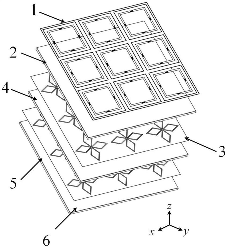
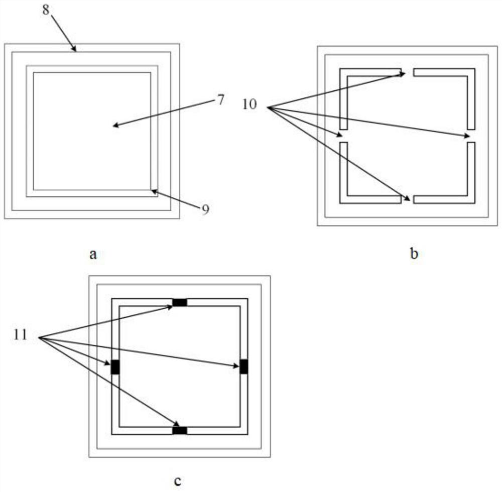
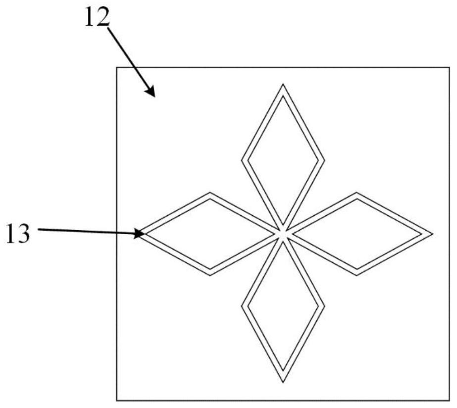
[0021] Such as Figure 1~3 As shown, a broadband high-power microwave adaptive protection device of the present invention includes a switch-type metasurface 1, an upper dielectric plate 2, a first band-pass frequency selective surface 3, a middle dielectric plate 4, The second bandpass frequency selective surface 5, the lower dielectric plate 6;
[0022] The switch-type metasurface 1 is printed on the upper surface of the upper dielectric plate 2, the first band-pass frequency selective surface 3 is printed on the upper surface of the middle dielectric plate 4, and the second band-pass frequency selective surface 5 is printed Made on the upper surface of the lower dielectric board 6, the middle of the upper dielectric board 2, the middle dielectric board 4 and the lower dielectric board 6 is an air layer, the centerline of the switch-type metasurface 1, the centerline of the upper dielectric board 2, The centerline of the first bandpass frequency selective surface 3, the cent...
PUM
 Abstract
Description
Claims
Application Information