Supercharge Your Innovation With Domain-Expert AI Agents!

Pulse width modulating switch power source and power supply control method thereof

A technology of pulse width modulation and switching power supply, which is applied in the direction of electrical components, output power conversion devices, and conversion of AC power input to DC power output. It can solve the problems of increasing switching energy loss, low power supply efficiency, and failure to achieve global optimization. problems, to achieve the effects of improving usage efficiency, optimizing power usage efficiency, and global optimization

Active Publication Date: 2013-01-16
LENOVO (BEIJING) LTD
View PDF0 Cites 0 Cited by
  • Summary
  • Abstract
  • Description
  • Claims
  • Application Information

AI Technical Summary

Problems solved by technology

[0014] In the case of high load of PWM switching power supply, the PWM switching power supply of MOSEFT parallel connection will lead to the increase of parasitic capacitance and increase the switching energy loss, but because the conduction energy loss dominates, the PWM switching power supply of MOSEFT parallel connection can effectively Reduce the conduction energy loss, so it can improve the power supply efficiency. However, compared with the low load, the switching energy loss dominates the energy loss of the PWM switching power supply. At this time, the PWM switching power supply of the MOSFET parallel mode reduces the conduction energy loss. , but the switching energy loss is increased, and because the switching energy loss is in a dominant position, the PWM switching power supply of the MOSFET parallel connection mode has low power supply efficiency under low load conditions
[0015] However, the PWM switching power supply using a single MOSFET has low power efficiency under high load conditions.
[0016] However, in general, once the switching power supply is designed, the circuit structure is fixed, but the power load is constantly changing, so the power efficiency of the existing PWM switching power supply is only a local optimization, and no global optimization has been achieved.

Method used


Image

  • Pulse width modulating switch power source and power supply control method thereof
  • Pulse width modulating switch power source and power supply control method thereof
  • Pulse width modulating switch power source and power supply control method thereof

Examples


Embodiment 1

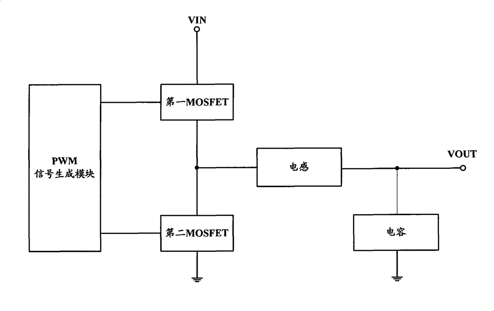
[0074] In the first embodiment, the case where the upper transistor is formed by two MOSFETs connected in parallel and the lower transistor is one MOSFET is described in detail.

[0075] The pulse width modulation switching power supply of the first embodiment of the present invention is as follows: image 3 shown, including:

[0076] a PWM controller, configured to generate and generate a first PWM signal and a second PWM signal that is inverted from the first PWM signal, and output the first PWM signal and the second PWM signal;

[0077] a MOSFET group including a first MOSFET, a second MOSFET and a third MOSFET;

[0078] A first MOSFET (Metallic Oxide Semiconductor Field Effect Transistor, Metal Oxide Semiconductor Field Effect Transistor) and a second MOSFET, the gates of the first MOSFET and the second MOSFET receive the first PWM signal and the second PWM signal ( That is, the gate of the first MOSFET is used to receive the first PWM signal, the gate of the second MOSF...

Embodiment 2

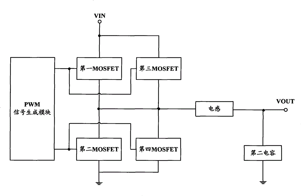
[0117] In the second embodiment, the case where two parallel-connected MOSFETs constitute the upper transistor and two parallel-connected MOSFETs constitute the lower transistor will be described in detail.

[0118] The pulse width modulation switching power supply of the second embodiment of the present invention is as follows: Figure 4 shown, including:

[0119] a PWM controller, configured to generate and generate a first PWM signal and a second PWM signal that is inverted from the first PWM signal, and output the first PWM signal and the second PWM signal;

[0120] a MOSFET group including a first MOSFET, a second MOSFET, a third MOSFET and a fourth MOSFET;

[0121] A first MOSFET (Metallic Oxide Semiconductor Field Effect Transistor, Metal Oxide Semiconductor Field Effect Transistor) and a second MOSFET, the gates of the first MOSFET and the second MOSFET respectively receive the first PWM signal and the second PWM signal, And the first terminal of the first MOSFET is ...

Embodiment 3

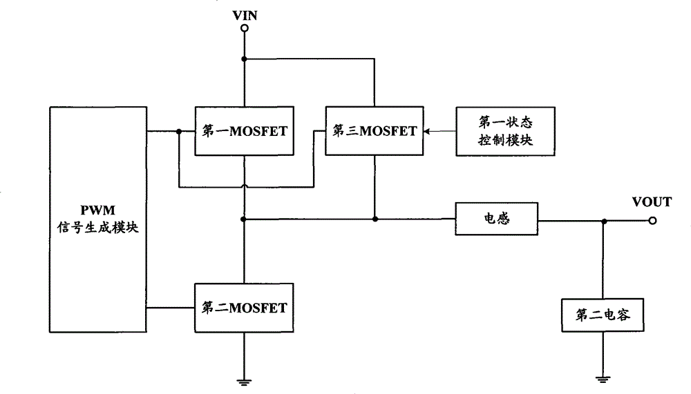
[0171] In the third embodiment, the case where at least three MOSFETs connected in parallel constitute the upper transistor and at least three MOSFETs connected in parallel constitute the lower transistor will be described in detail.

[0172] The pulse width modulation switching power supply of the third embodiment of the present invention is as follows: Figure 5 As shown, considering the simplicity of the figure, the FETs in the figure represent MOSFETs, including:

[0173] a PWM controller, configured to generate and generate a first PWM signal and a second PWM signal that is inverted from the first PWM signal, and output the first PWM signal and the second PWM signal;

[0174] a MOSFET group comprising a first MOSFET, a second MOSFET, a first set of MOSFETs, and a second set of MOSFETs;

[0175] A first MOSFET (Metallic Oxide Semiconductor Field Effect Transistor, Metal Oxide Semiconductor Field Effect Transistor) and a second MOSFET, the gates of the first MOSFET and the...


PUM


Abstract

The invention provides a pulse width modulating PWM switch power source which solves the problem that the efficiency of a PWM power source in the prior art is locally optimized. The switch power source comprises a pulse width modulating PWM controller and MOSFET group, wherein the MOSFET group also comprises at least one controlled MOSFET, and the at least one controlled MOSFET is connected with a first MOSFET or a second MOSFET in parallel; and the pulse width modulating PWM switch power source also comprises a state control module which controls the working condition of the at least one controlled MOSFET according to the control parameter to convert the first working condition of the MOSFET group to the second working condition, thus lowering the total power loss of the MOSFET group. The invention improves the switch power source efficiency and realizes overall optimal efficiency.

Description

technical field [0001] The invention relates to the technical field of switching power supplies, in particular to a pulse width modulation switching power supply and a power supply control method thereof. Background technique [0002] With the development of the chip manufacturing process, more and more switching power supplies are implemented using PWM (Pulse Wide Modulation, pulse width modulation). [0003] A switching power supply implemented using PWM such as figure 1 shown, including: [0004] a PWM controller that generates a first PWM signal and a second PWM signal that is inverted from the first PWM signal; [0005] A first MOSFET (Metallic Oxide Semiconductor Field Effect Transistor, Metal Oxide Semiconductor Field Effect Transistor) and a second MOSFET, the gates of the first MOSFET and the second MOSFET respectively receive the first PWM signal and the second PWM signal, And the first terminal of the first MOSFET is connected to the power input terminal, the s...

Claims


Application Information

Patent Timeline
Patent Type & Authority Patents(China)
IPC IPC(8): H02M7/523H02M7/527
Inventor 张敏
Owner LENOVO (BEIJING) LTD
Features
  • R&D
  • Intellectual Property
  • Life Sciences
  • Materials
  • Tech Scout
  • Unparalleled Data Quality
  • Higher Quality Content
  • 60% Fewer Hallucinations
Learn More