Method for producing an electronic component and electronic component

A technology for electronic components and components, which is applied in the manufacture of electrical components, electric solid-state devices, semiconductor/solid-state devices, etc., can solve the problems of high cost and high-cost cleaning process, and achieve the effect of simple insulating layer and avoiding weak links.

Inactive Publication Date: 2010-06-30
SIEMENS AG
View PDF0 Cites 2 Cited by
  • Summary
  • Abstract
  • Description
  • Claims
  • Application Information

AI Technical Summary

Problems solved by technology

The laser ablation process is very costly and causes laser smoke formation, resulting in costly cleaning processes

Method used


Image

  • Method for producing an electronic component and electronic component
  • Method for producing an electronic component and electronic component
  • Method for producing an electronic component and electronic component

Examples


Embodiment Construction

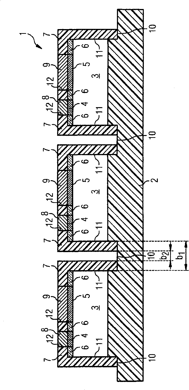
[0035] figure 1 A schematic illustration shows a cross-section of, for example, three chips arranged side by side in composite wafer 1 . In this case, the chip 3 is arranged on a carrier 2, for example a serrated film equipped with an adhesive surface. In this case, the connection of the carrier 2 to the wafer takes place before the chip 3 is separated from the composite wafer 1 .

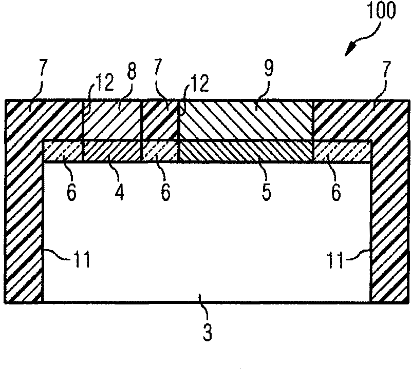
[0036] Each of the chips 3 has, for example, two chip contact areas 4 , 5 on the main side facing away from the carrier 2 . These main sides are provided with a passivation layer 6 as usual when processing wafers. In a known manner, the chip contact areas 4 , 5 and the surface of the passivation layer 6 facing away from the chip 3 lie approximately in one plane.

[0037] As a preparation for applying the insulating layer 7 to the surfaces of the chips 3 , the chips 3 are optionally (adhered to the carrier 2 ) separated from one another. The width of each corresponding dividing line between two ...


PUM

PropertyMeasurementUnit
Layer thicknessaaaaaaaaaa
Thicknessaaaaaaaaaa

Abstract

The invention relates to a method for producing an electronic component (100), wherein a plurality of chips (3) disposed in a wafer on a passivated main side having at least one chip contact surface (4, 5) is provided with an insulation layer (7). The insulation layer (7) has openings (12) in the area of the at least one chip contact surface (4, 5) of each chip (3). The chip contact surfaces (4, 5) of each chip (3) are provided with a chip contact surface metallization (8, 9) of a prescribed thickness, and the chips disposed in the wafer (3) are separated therefrom.

Description

technical field [0001] The invention relates to a method for producing an electronic component and to an electronic component. Background technique [0002] Electronic components generally comprise a carrier or a substrate to which a structured metal layer with metal surfaces or contact surfaces is applied. Some of these contact surfaces are each coated with one or more components, for example semiconductor chips or passive components. The one or more devices are connected to the respective contact surfaces by a connecting medium, usually solder. If one of the components has a backside contact, ie a contact facing the carrier or the substrate, then not only a mechanical but also an electrical connection to the respective contact surface is established via the connecting medium. In the case of an electrical contact connection, at least some of the components each have a plurality of contact areas on their upper side facing away from the carrier. The electrical connection o...

Claims


Application Information

Patent Timeline
IPC IPC(8): H01L23/31H01L21/56H01L23/482H01L21/60
CPCH01L2924/01005H01L2224/24225H01L2924/01082H01L21/561H01L24/82H01L24/24H01L2924/01023H01L2224/82102H01L2224/76155H01L2924/01029H01L23/3185H01L2224/24226H01L2924/19043H01L2924/01006H01L21/6835H01L2924/01033H01L21/568H01L2924/0102H01L2224/24051H01L2924/12041H01L2224/0603H01L2924/00
Inventor K·韦德纳W·霍夫曼R·霍弗H·施瓦茨鲍尔
Owner SIEMENS AG
Why Eureka
Try Eureka