Membrane device with electromagnetic interference resisting and signal receiving and transmitting functions and molding method

A technology for preventing electromagnetic waves and forming methods, which is applied to circuits, electrical components, magnetic field/electric field shielding, etc.

Inactive Publication Date: 2010-07-28
PARAGON TECH
View PDF0 Cites 0 Cited by
  • Summary
  • Abstract
  • Description
  • Claims
  • Application Information

AI Technical Summary

Problems solved by technology

[0003] In order to adapt to the development trend of today's light, thin and small products, the components of each part of the electronic equipment must be relatively reduced in size, and the antenna is no exception. In terms of existing technology, the antenna can not only be set into a three-dimensional plate frame type In addition, it has been able to be further made into a sheet state, so its volume reduction is not a problem; however, in the design of electronic equipment for the stability of antenna transmission and reception signals, in order to prevent the external emission of magnetic waves generated by the internal electronic components of the equipment. Signal interference is usually overcome by installing an additional shielding metal. Taking the structure of a notebook computer as an example, the common method is to take a metal plate and lock it inside the housing on the side of the LCD panel. There are also metal foils in the industry. However, this kind of common practice is obviously still too complicated, resulting in the disadvantages and problems that the overall antenna-related structure still has to go through multiple processes before it can be completed, which obviously fails to meet the ultimate expectations of the relevant industries. How to develop The innovative design that can simplify the manufacturing process and further reduce the cost is obviously the goal and direction that the relevant industries are looking forward to and must work hard to think about in the current fierce market environment.

Method used


Image

  • Membrane device with electromagnetic interference resisting and signal receiving and transmitting functions and molding method
  • Membrane device with electromagnetic interference resisting and signal receiving and transmitting functions and molding method
  • Membrane device with electromagnetic interference resisting and signal receiving and transmitting functions and molding method

Examples


Embodiment Construction

[0024] Embodiments of the present invention will be described in detail below in conjunction with the accompanying drawings.

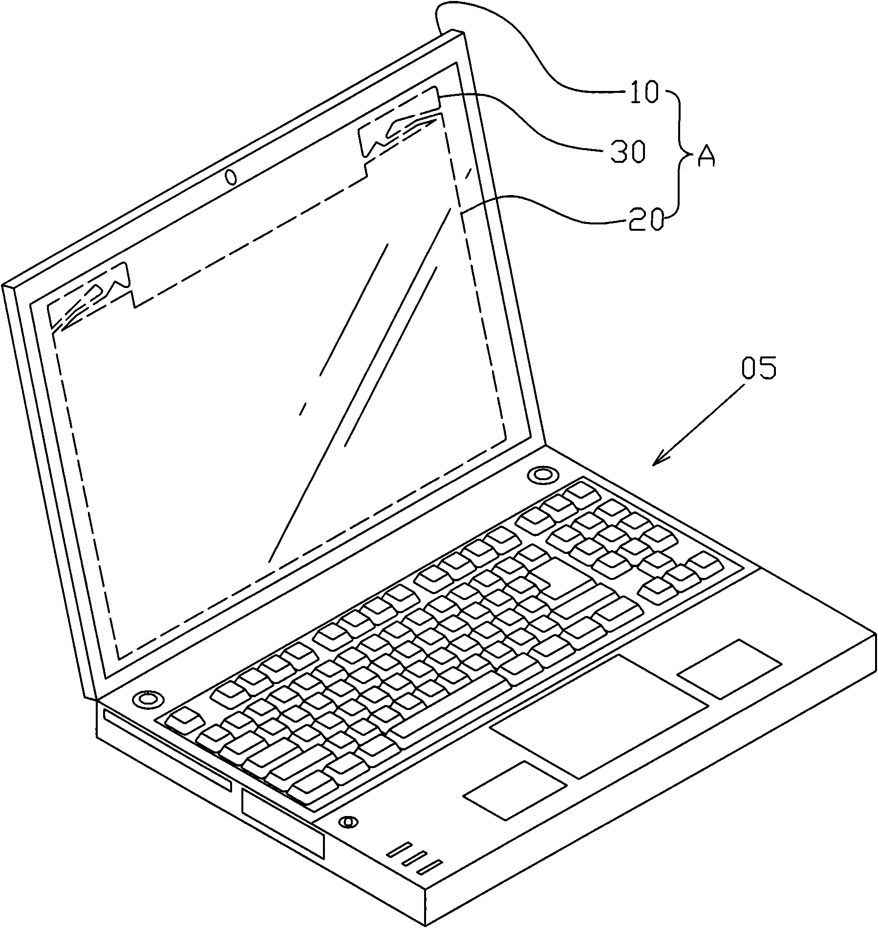
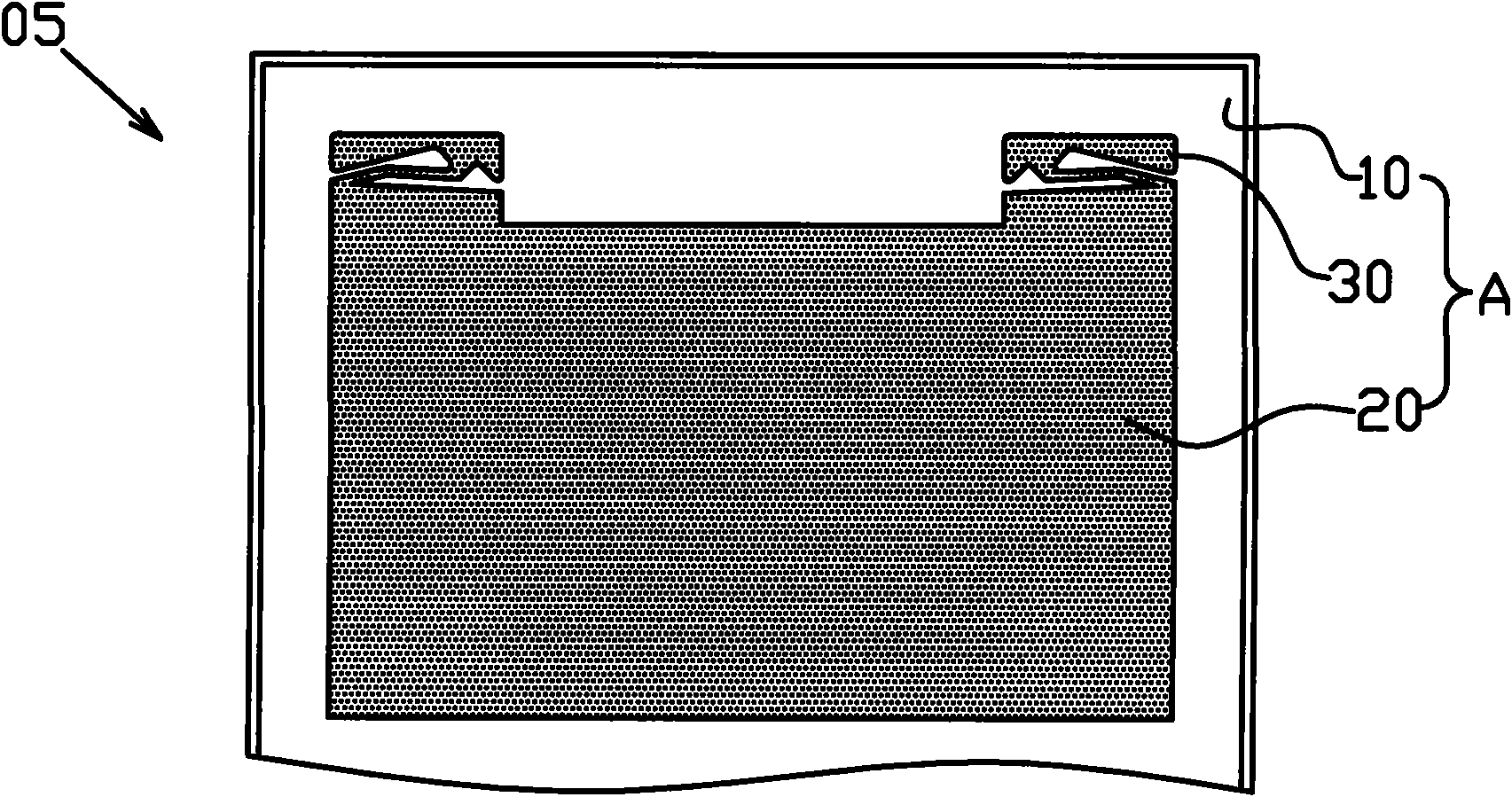
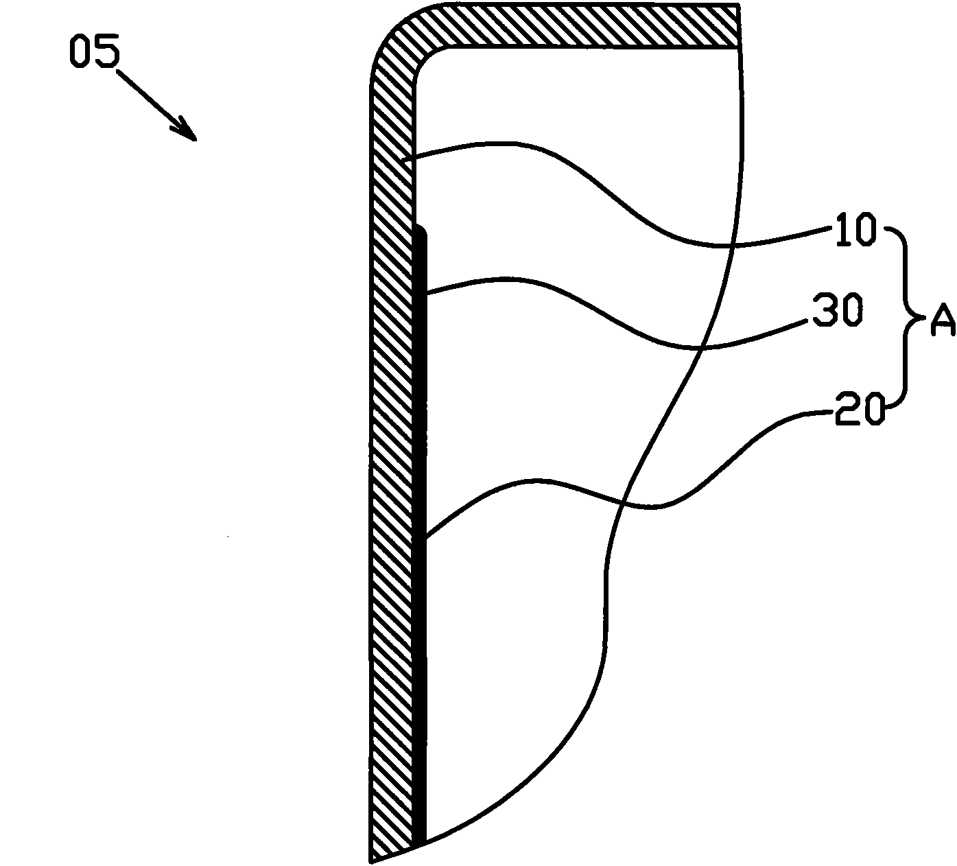
[0025] see figure 1 and figure 2 , which is a preferred embodiment of the thin film device and forming method with the functions of anti-electromagnetic interference and signal transmission and reception of the present invention, all embodiments are for illustration purposes only, and are not limited by this structure in patent application.

[0026] The thin-film device A having the functions of preventing electromagnetic interference and transmitting and receiving signals includes the following components:

[0027] A base material 10, the base material 10 can be the casing or internal components of the electronic device 05 (such as a support frame plate, a component substrate, etc.), so the base material 10 is not limited to a flat plate, an arc surface, a curved surface , Concave and convex surfaces are all within the defined range; and the electr...


PUM


Abstract

The invention discloses a membrane device with electromagnetic interference resisting and signal receiving and transmitting functions and a molding method. The membrane device comprises a substrate material, a conductive thin layer, and a signal receiving and transmitting part, wherein the conductive thin layer is integrally attached to a position on which the substrate is arranged and is in the form of a thin layer. The method comprises the following steps of: selecting the substrate material; selecting a signal receiving and transmitting mode and a conductive metal surface mode according to a required working frequency band; and forming the signal receiving and transmitting part in the form of the thin layer and the conductive thin layer on a region in which the substrate is arranged by means of attachment. Therefore, the conductive thin layer with signal receiving and transmitting and shielding effects can be formed on the substrate by attachment means such as film coating and spraying, the assembling procedure of a signal receiving and transmitting device of an electronic device can be simplified greatly, the production efficiency is enhanced, the cost is saved, and the advancement of the shielding effect and excellent industrial economic benefit are achieved. The invention can be suitable for various occasions and situations which need the membrane device with the electromagnetic interference resisting and signal receiving and transmitting functions and the molding method.

Description

technical field [0001] The invention relates to a device for communication electronic equipment, in particular to a thin-film device and a molding method with a thin-layered signal transceiving part and a conductive thin layer attached to the surface of a substrate, which have both anti-electromagnetic interference and signal transceiving functions. Background technique [0002] With the vigorous development of information technology and the Internet, electronic devices such as notebook computers, personal digital assistants (PDAs), mobile phones, satellite navigation devices, etc., have introduced wireless transmission functions to achieve more freedom of communication and Internet access. The purpose of space limitation; and the important component to achieve the wireless transmission function, the antenna is obviously the protagonist and there is no doubt. [0003] In order to adapt to the development trend of today's light, thin and small products, the components of each...

Claims


Application Information

Patent Timeline
Patent Type & Authority Applications(China)
IPC IPC(8): H05K9/00H01Q1/00H05K7/00
Inventor 陈忠汉田茂良郑平熙李骏扬
Owner PARAGON TECH
Why Eureka
Try Eureka