Circuit for lowering CMOS transient power consumption

A technology of transient power consumption and MOS transistors, which is applied in the field of micro-nano electronics, can solve problems such as deviation of simulation results, achieve the effects of reducing transient current, eliminating feedthrough channels, and reducing transient power consumption

Active Publication Date: 2010-08-04
SHANGHAI INST OF MICROSYSTEM & INFORMATION TECH CHINESE ACAD OF SCI
View PDF4 Cites 2 Cited by
  • Summary
  • Abstract
  • Description
  • Claims
  • Application Information

AI Technical Summary

Problems solved by technology

But since the bias current used is only 100nA
According to theory, the transient current should be kept constant at around 100nA, but the simulation results deviate greatly from the theory

Method used


Image

  • Circuit for lowering CMOS transient power consumption
  • Circuit for lowering CMOS transient power consumption
  • Circuit for lowering CMOS transient power consumption

Examples


Embodiment Construction

[0017] The specific implementation manner of the present invention will be further described below by taking a traditional CMOS gate circuit-inverter as an example in conjunction with the accompanying drawings.

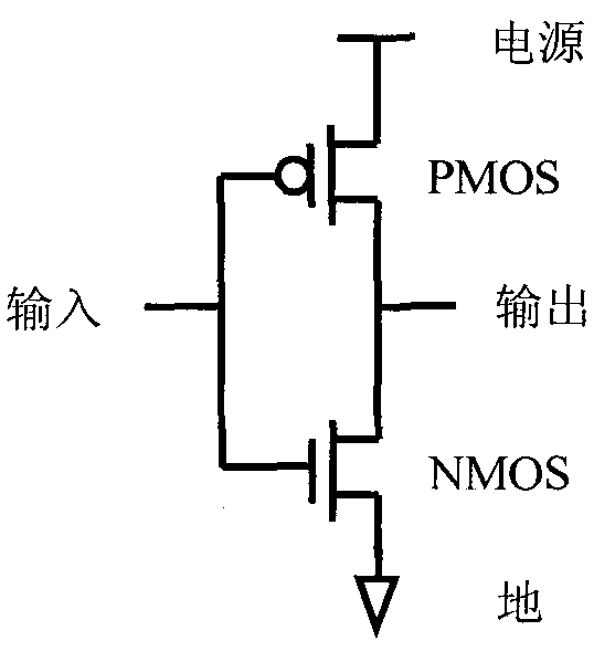
[0018] Please see image 3 A circuit for reducing CMOS transient power consumption of the present invention includes a CMOS inverter formed by connecting a PMOS transistor P1 and an NMOS transistor N1. The PMOS transistor used is provided with a source, a drain, a gate and a base drawn out from its substrate common well (N well). The gate of the PMOS transistor P1 is connected to the gate of the NMOS transistor N1 and is an input terminal; the drain of the PMOS transistor P1 is connected to the source of the NMOS transistor N1 and is an output terminal; the source of the PMOS transistor P1 is connected to a high level , that is, the power supply level is connected; the drain of the NMOS transistor N1 is grounded.

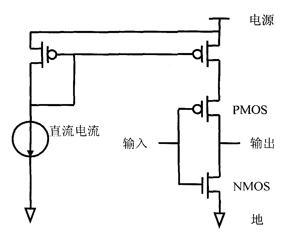
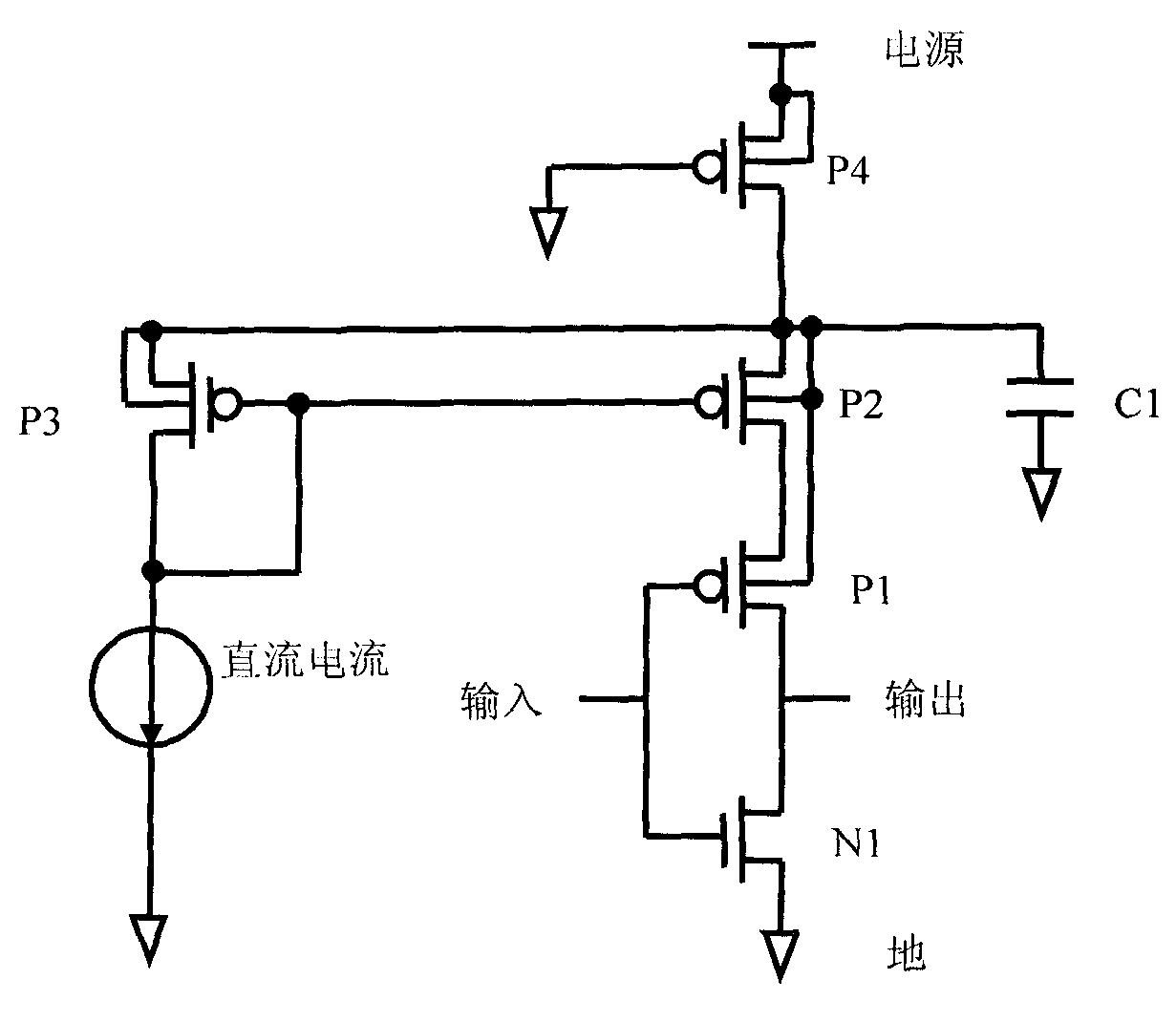
[0019] In order to limit the transient current of t...


PUM


Abstract

The invention relates to a circuit for lowering CMOS transient power consumption, comprising a CMOS gate circuit composed of a PMOS transistor and an NMOS transistor, wherein the source electrode of the NMOS transistor is accessed to a power supply level; a barrier device is inserted between a base electrode and a power supply of the PMOS transistor of the pull-up network of a gate circuit to isolate the base electrode from the power supply end; and a voltage regulator is added on the base electrode to enable the voltage value of the base electrode to be constant in a certain range. Thus, in the process of switching input signals of the gate circuit, feed-through current flowing from the power supply to an input end via the base electrode is avoided, thus lowering transient power consumption of a CMOS integrated circuit, and ensuring the base electrode level to be unchangeable without influencing operation of the logic gate circuit due to the voltage regulator.

Description

technical field [0001] The invention relates to a CMOS integrated circuit, in particular to a circuit for reducing the transient power consumption of the CMOS integrated circuit. The invention belongs to the technical field of micro-nano electronics. Background technique [0002] There are two main sources of power consumption for ordinary CMOS gate circuits: one is called static power consumption; the other is dynamic power consumption. Static power consumption refers to the power consumption caused by the leakage current from the power supply terminal to the ground when the input terminal of the CMOS gate circuit is kept constant. Dynamic power consumption refers to the power consumption caused by the instantaneous change of the input terminal of the CMOS gate circuit. When the input terminal of the CMOS gate circuit changes, the pull-up network and the pull-down network of the gate circuit must be turned on at the same time, causing a large transient current to flow fro...

Claims


Application Information

Patent Timeline
Patent Type & Authority Applications(China)
IPC IPC(8): H03K19/20
Inventor 丁晟宋志棠陈后鹏
Owner SHANGHAI INST OF MICROSYSTEM & INFORMATION TECH CHINESE ACAD OF SCI
Why Eureka
Try Eureka