Communication chip system chip tracing and debugging method and apparatus

A system-on-chip and communication technology, applied in the field of communication, can solve problems such as high overhead, information loss, and inability to locate, and achieve the effects of fast recording, low overhead, and low software overhead

Inactive Publication Date: 2009-07-29
ZTE CORP
View PDF0 Cites 14 Cited by
  • Summary
  • Abstract
  • Description
  • Claims
  • Application Information

AI Technical Summary

Problems solved by technology

This method can record information in a targeted manner, but the overhead is too large and the speed is slow, which has a certain impact on the operation of the original system
And when a fatal error occurs in the software, the original information is lost and the problem cannot be located

Method used


Image

  • Communication chip system chip tracing and debugging method and apparatus
  • Communication chip system chip tracing and debugging method and apparatus
  • Communication chip system chip tracing and debugging method and apparatus

Examples


Embodiment Construction

[0047] The present invention will be further described below in conjunction with the accompanying drawings and specific embodiments.

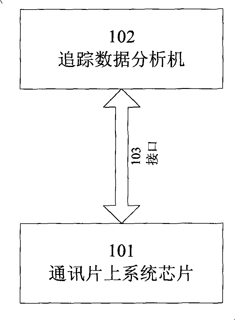
[0048] The overall schematic diagram of the device used in the method for tracking, debugging and analyzing the chip on chip of the communication system in the present invention is shown in figure 1 , consisting of 101, 102, 103, wherein 101 is a communication SoC chip; the tracking data analysis machine 102 can be an embedded processor, or a common PC (personal computer); 103 is an interface, which is a SoC chip and tracking data The channel through which the analysis machine transmits debugging data can be a serial port, a USB port, or a LAN interface, etc., which can be determined according to the existing interfaces of the actual system.

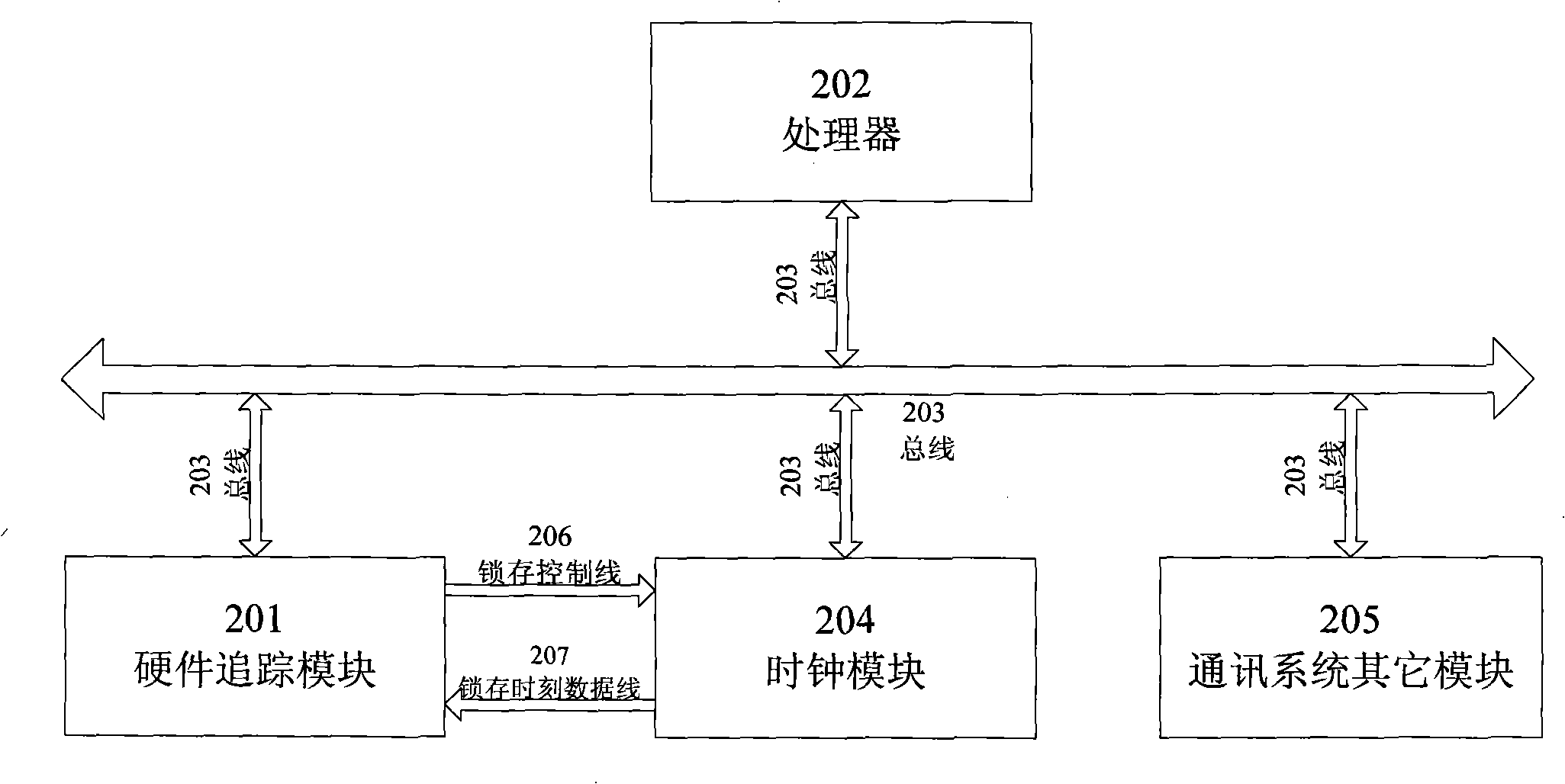
[0049] For the overall architecture diagram of the communication system-on-chip with a hardware tracking module, please refer to figure 2 ,Depend on figure 2201, 202, 203, 204, 205, 206, and 207 consi...


PUM


Abstract

The invention discloses a method and a device for tracing and debugging a system chip of a communication chip, wherein, the system chip of the communication chip comprises a hardware tracking module. The method has the following steps: firstly, the trace and debug data is written and stored in the hardware tracking module, and then output to a track data analysis machine which stores the track and debug data and then analyses and processes the track and debug data to determine the problem of the system. The method and the device collects the data in debugging in batch according to the demand of design, reduces the cost of software of the original system, is more similar to the real system, can automatically sore the very important system time information in the communication system while in the process of recording the track and debug date, help the designer to effectively understand and analyze the integral process of the system by automatic software analysis, determine the problem more rapidly, save workload of the design staff, and improve the work efficiency.

Description

technical field [0001] The invention relates to the field of communication, in particular to a method and device for tracking and debugging a system-on-chip communication chip. Background technique [0002] Related chips of current communication systems, including system-side and terminal-side chips, are usually more complex, and are generally designed as SoCs, including both hardware design and software design. [0003] The system of the SoC chip is relatively large, and its design and debugging involve many modules and are relatively complicated. For tracking complex software faults such as software runaway, there are two traditional tracking and debugging methods. One of the methods is to use the ICE debugging tool that comes with the processor to record all instructions for analysis. All the instructions run by the processor are recorded, the amount of information is too large, and the records are not focused. It is useful to analyze the problems in the design of the so...

Claims


Application Information

Patent Timeline
Patent Type & Authority Applications(China)
IPC IPC(8): G06F17/50G06F11/36
Inventor 夏长松
Owner ZTE CORP
Why Eureka
Try Eureka