Pixel structure and maintenance method thereof

A technology of pixel structure and pixel unit, applied in nonlinear optics, instruments, optics, etc., can solve the problems of complex maintenance process and damage to common electrode lines, and achieve the effect of simple maintenance process

Active Publication Date: 2011-11-09
BOE TECH GRP CO LTD +1
View PDF0 Cites 0 Cited by
  • Summary
  • Abstract
  • Description
  • Claims
  • Application Information

AI Technical Summary

Problems solved by technology

[0007] In the above-mentioned maintenance process, if the deposited metal line crosses the common electrode line 16, the pixel electrode 9 on the upper part of the common electrode line 16 cannot be cut with a high-energy laser, otherwise the common electrode line 16 will be destroyed, so the pixel is cut at the end here. For electrode 9, it is necessary to use a laser with a lower energy, which makes the whole maintenance process more complicated
[0008] Since the above two cases include welding operation, cutting operation and wiring operation at the same time, for the cutting operation that needs to cross the common electrode line, it is necessary to use a laser with a smaller energy (called decap operation); since the welding operation and the cutting operation are the same maintenance equipment On, while the wiring operation and decap operation need to be in another maintenance equipment It is carried out on the computer, so the maintenance process is more complicated, and the maintenance equipment needs to be replaced

Method used


Image

  • Pixel structure and maintenance method thereof
  • Pixel structure and maintenance method thereof
  • Pixel structure and maintenance method thereof

Examples


Embodiment 1

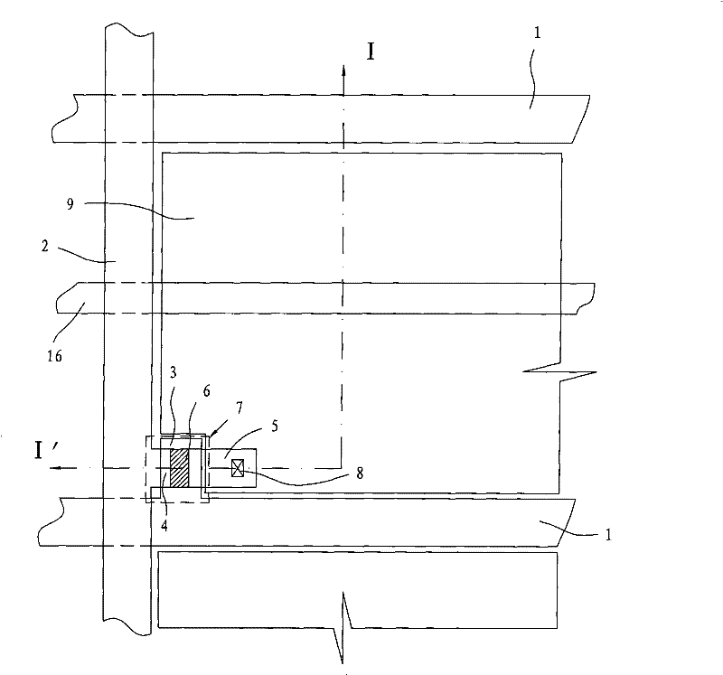
[0033] An embodiment of the present invention provides a pixel structure, such as Figure 5 As shown, the pixel structure includes gate scan lines 420 , 450 and data scan lines 410 intersecting each other on a substrate 470 , and the intersections of the gate scan lines 450 and data scan lines 410 define pixel units.

[0034] In order to facilitate maintenance after the data scanning line is disconnected, the pixel structure of the embodiment of the present invention also needs to set a light shielding part, which is a closed structure and connected to the gate scanning line 450, and the light shielding part and the gate scanning line 450 are located at the same layer. Specifically, as Figure 6 As shown, the light-shielding portion includes vertical light-shielding strips 460 and horizontal light-shielding strips 461 parallel to the data scanning lines. The specific arrangement of the vertical light-shielding strip 460 is as follows: vertical light-shielding strips 460 resp...

Embodiment 2

[0041] The embodiment of the present invention also provides a method for repairing the pixel structure, the repair method is mainly aimed at the following two situations:

[0042] First, the data scanning line at the corresponding position between the two ends of the shading strip is disconnected.

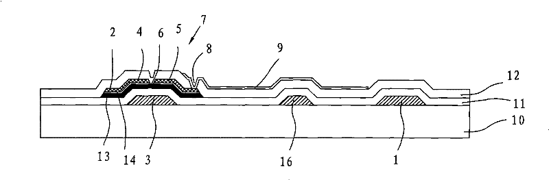
[0043] For the maintenance under this situation, the specific operation of the embodiment of the present invention is as follows: Figure 7 As shown, holes 510 and 511 are punched at the overlapping position of the data scanning line 410 and the horizontal light-shielding strip. Filling with metal (that is, welding operation); in this way, the horizontal light-shielding strips of the light-shielding portion and the data scanning lines 410 are connected together through the metal in the holes 510 and 511, so that the disconnected data scanning lines 410 are connected through the light-shielding portion.

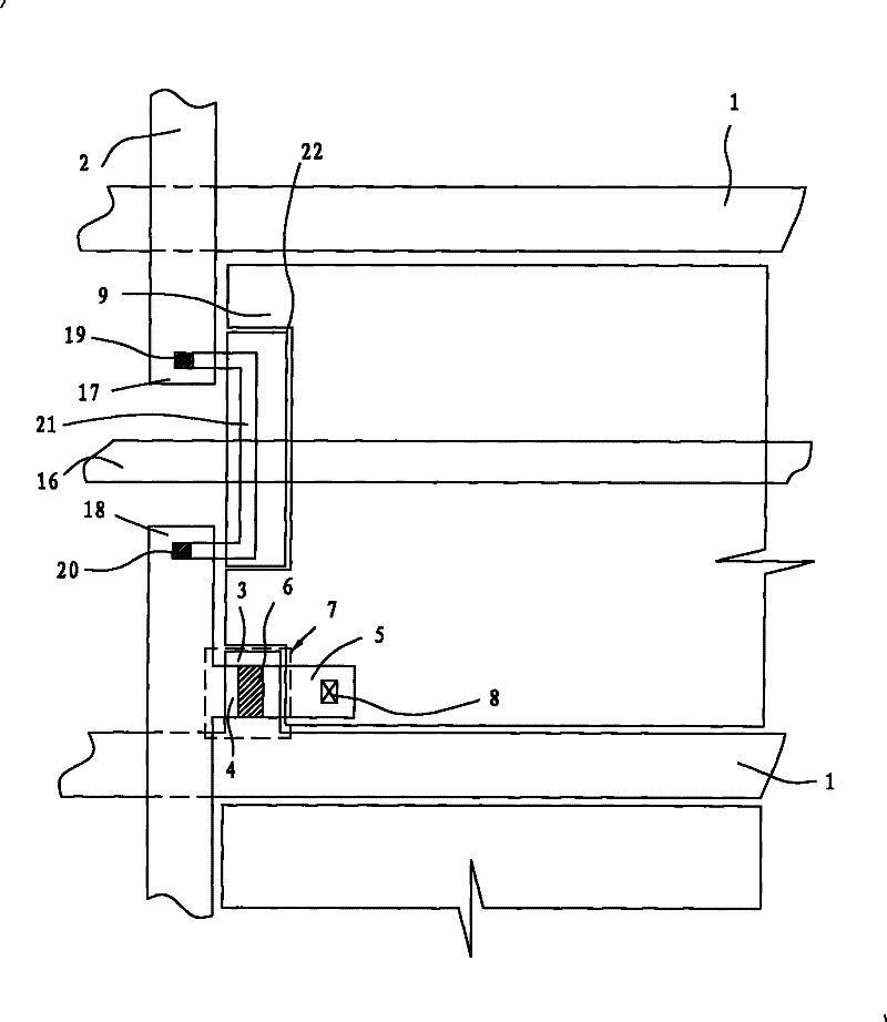
[0044] If the vertical light-shielding strip 460 in the present invention is...


PUM


Abstract

The invention discloses a pixel structure and a maintenance method thereof, which relates to the technical field of liquid crystal display and solves the problems of complex maintenance progress and necessary maintenance device replacement for the traditional pixel structure. The invention embodiment is provided with a light shading part corresponding to data scanning lines on a grid and a grid layer of grid scanning lines. The light shading part is of a sealed structure and is connected to the grid scanning lines. The invention embodiment is mainly applied to the liquid crystal display, in particular to the liquid crystal display adopting TFT manufacture technology.

Description

technical field [0001] The invention relates to the technical field of liquid crystal displays, in particular to a pixel structure of a liquid crystal display and a repair method for defective lines of the pixel structure. Background technique [0002] Such as figure 1 and figure 2 As shown, the TFT array substrate includes a gate scanning line 1 and a data scanning line 2 arranged on the lower substrate to cross each other, and a TFT 7 and a pixel electrode 9 are arranged in each area formed by the intersection of the gate scanning line 1 and the data scanning line 2 and the common electrode line 16. For the specific structure of TFT7, see figure 2 The TFT sectional view shown, the TFT7 includes a gate 3 connected to the gate scanning line 1, a source 4 connected to the data scanning line 2, and a drain 5 connected to the pixel electrode 9, wherein the drain 5 passes through the contact hole 8 is connected to the pixel electrode 9; the TFT 7 also includes a semiconduc...

Claims


Application Information

Patent Timeline
Patent Type & Authority Patents(China)
IPC IPC(8): G02F1/1362G02F1/13
Inventor 陈宇鹏
Owner BOE TECH GRP CO LTD
Why Eureka
Try Eureka