AI technical title is built by PatSnap AI team. It summarizes the technical point description of the patent document.
A chip-bonding film and cutting film technology, applied in the direction of pressure-sensitive film/sheet, polyurea/polyurethane adhesive, film/sheet-shaped adhesive, etc., can solve the problem of not being able to easily pick up semiconductor chips, difficult to obtain cutting/ Die-bonding film, large area, etc., to achieve the effect of preventing the disappearance of the boundary surface, good pick-up, and realizing the peeling force
Active Publication Date: 2010-10-06
NITTO DENKO CORP
View PDF3 Cites 4 Cited by
Summary
Abstract
Description
Claims
Application Information
AI Technical Summary
This helps you quickly interpret patents by identifying the three key elements:
Problems solved by technology
Method used
Benefits of technology
Problems solved by technology
[0006] However, even with this improved method, it may be difficult to obtain a dicing / die-bonding film that has a good balance between the holding force during dicing and the subsequent peelability.
For example, when obtaining a large semiconductor chip of 10mm x 10mm or more, the semiconductor chip cannot be easily picked up by a general die bonder due to its large area
Method used
Image
Click on the blue label to locate the original text in one second.
Reading with bidirectional positioning of images and text.
Examples
Embodiment 1
[0097]
[0098] In a reaction vessel with a condenser tube, a nitrogen inlet tube, a thermometer and a stirring device, add 88.8 parts of 2-ethylhexyl acrylate (hereinafter referred to as "2EHA"), 11.2 parts of 2-hydroxyethyl acrylate (hereinafter referred to as "HEA"), 0.2 parts of benzoyl peroxide, and 65 parts of toluene were polymerized in a nitrogen stream at 61° C. for 6 hours to obtain an acrylic polymer A with a weight average molecular weight of 850,000. The weight average molecular weight is as follows. The molar ratio of 2EHA to HEA is 100 moles: 20 moles.
[0099] 12 parts (80 mol% with respect to HEA) of 2-methacryloyloxyethyl isocyanate (hereinafter referred to as "MOI") was added to this acrylic polymer A, and the process was carried out at 50° C. for 48 hours in an air stream. Addition reaction treatment gave acrylic polymer A'.
[0100] Then, 8 parts of polyisocyanate compound (trade name "Coroneto L", manufactured by Nippon Polyurethane Co., Ltd.) and 5 p...
Embodiment 2~15
[0116] In each of Examples 2-15, except having changed into the composition and content shown in following Table 1, it carried out similarly to said Example 1, and produced the dicing / die-bonding film.
[0117]
[0118] In addition, the meanings of the abbreviations described in Table 1 and Table 2 described later are as follows.
[0119] 2EHA: 2-Ethylhexyl Acrylate
[0120] i-OA: Isooctyl acrylate
[0121] i-NA: Isononyl Acrylate
[0122] BA: n-butyl acrylate
[0123] LA: lauryl acrylate
[0124] AA: Acrylic
[0125] HEA: 2-Hydroxyethyl Acrylate
[0126] 4HBA: 4-Hydroxybutyl Acrylate
[0127] AOI: 2-acryloyloxyethyl isocyanate
[0128] C / L: polyisocyanate compound (trade name "Coroneto L", manufactured by Nippon Polyurethane Co., Ltd.)
[0129] T / C: Epoxy crosslinking agent (trade name "Tetrade C", manufactured by Mitsubishi Gas Chemical Co., Ltd.)
PUM
Property
Measurement
Unit
thickness
aaaaa
aaaaa
Abstract
Disclosed is a dicing die-bonding film which has an excellent balance between a holding force during the dicing of a work and detachability upon the detachment of a chip-type work produced by the dicing together with the die-bonding film even when the work is thin. The dicing die-bonding film comprises a base material, a dicing film arranged on the base material and having an adhesive layer, and a die-bonding film arranged on the adhesive layer, wherein the adhesive layer comprises a polymer comprising an acrylic acid ester as the main monomer, a hydroxyl-containing monomer at a content of 10 to 30 mol% relative to the amount of the acrylic acid ester, and an isocyanate compound having a radical-reactive carbon-carbon double bond at a content of 70 to 90 mol% relative to the amount of the hydroxyl-containing monomer, and wherein the die-bonding film comprises an epoxy resin.
Description
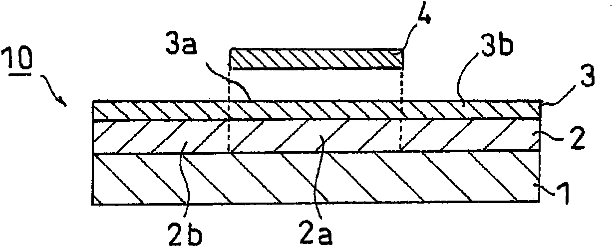
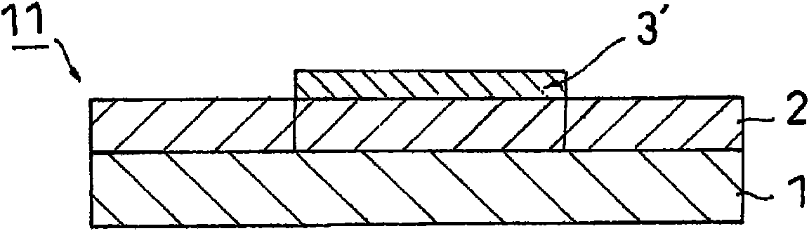
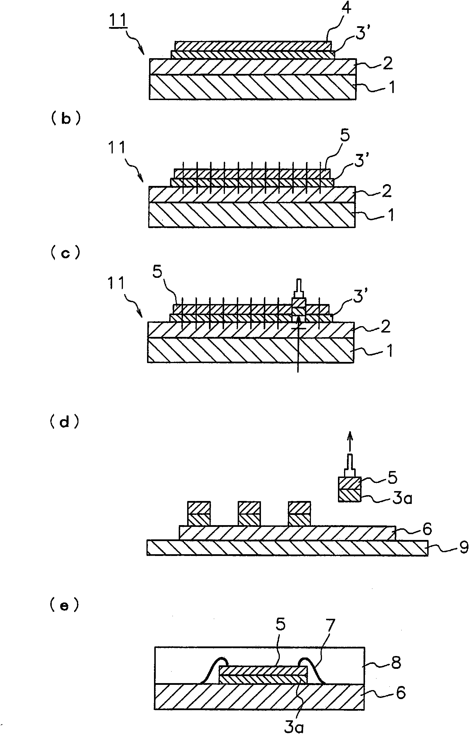
technical field [0001] The present invention relates to a dicing / die-bonding film in which an adhesive for fixing a chip-shaped workpiece (semiconductor chip, etc.) and an electrode member is attached to the workpiece (semiconductor wafer, etc.) before dicing and supplied to the workpiece for dicing. Background technique [0002] The semiconductor wafer (work) on which the circuit pattern is formed is diced into semiconductor chips (chip-shaped workpieces) after the thickness is adjusted by back grinding as necessary (dicing process). In the cutting process, in order to remove the cutting layer, generally under moderate hydraulic pressure (usually about 2kg / cm 2 ) to clean the semiconductor wafer. Then, after the aforementioned semiconductor chip is fixed to an adherend such as a lead frame with an adhesive (mounting step), the process proceeds to a bonding step. In the mounting process, an adhesive is applied to a lead frame or a semiconductor chip. However, in this meth...
Claims
Application Information
Patent Timeline
Application Date:The date an application was filed.
Publication Date:The date a patent or application was officially published.
First Publication Date:The earliest publication date of a patent with the same application number.
Issue Date:Publication date of the patent grant document.
PCT Entry Date:The Entry date of PCT National Phase.
Estimated Expiry Date:The statutory expiry date of a patent right according to the Patent Law, and it is the longest term of protection that the patent right can achieve without the termination of the patent right due to other reasons(Term extension factor has been taken into account ).
Invalid Date:Actual expiry date is based on effective date or publication date of legal transaction data of invalid patent.

