

Sub-pixel structure and liquid crystal display panel
A liquid crystal display panel and liquid crystal display technology, applied in static indicators, nonlinear optics, instruments, etc., can solve problems such as insufficient charging capacity, achieve the effect of improving color shift and increasing charging time
- Summary
- Abstract
- Description
- Claims
- Application Information
AI Technical Summary
Problems solved by technology
Method used
Image

Examples
Embodiment Construction
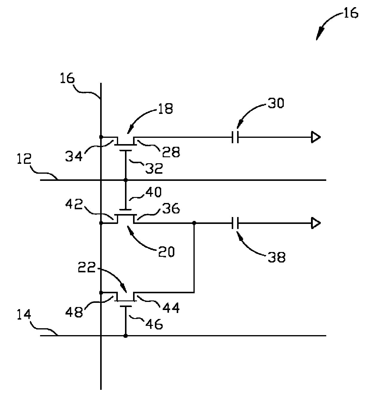
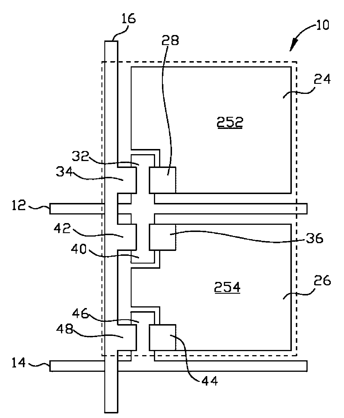
[0018] Please refer to figure 1 and figure 2 , figure 1 A pixel equivalent circuit diagram in which three thin film transistors are arranged in a sub-pixel structure for the first embodiment of the present invention, figure 2 Then it is the pixel schematic diagram of the sub-pixel structure in Fig. 1 . As shown in the figure, the sub-pixel structure 10 of the thin film transistor liquid crystal display of the present invention can be arranged between a color filter substrate and a thin film transistor substrate, and each sub-pixel structure 10 includes two scanning lines arranged horizontally 12 , 14 , a data line 16 vertically intersecting the scan lines 12 , 14 and three thin film transistors 18 , 20 , 22 are electrically connected to the scan lines 12 , 14 and the data line 16 respectively. Wherein, the thin film transistors 18, 20, 22 can be a bottom gate (Bottom Gate) structure or an upper gate (Top Gate) structure, and each sub-pixel structure 10 includes two parts,...
PUM
 Abstract
Description
Claims
Application Information