
Transmission system for image display device and electronic equipment

一种图像显示装置、传输系统的技术,应用在辨认装置、静态指示器、光导等方向,达到简单结构、价格低廉、避免EMI的效果

Inactive Publication Date: 2010-11-17
SHARP KK
View PDF3 Cites 1 Cited by
  • Summary
  • Abstract
  • Description
  • Claims
  • Application Information

AI Technical Summary

Problems solved by technology

Therefore, for a flexible substrate that transmits high-speed signals between the image processing IC and the image display driver IC, and is curved during use, the influence of impedance mismatch is particularly significant, and there is a possibility that electromagnetic noise is radiated to other devices. Problems (EMI) and problems with other equipment picking up noise components (EMS)
These become big problems in achieving high resolution

Method used


Image

  • Transmission system for image display device and electronic equipment
  • Transmission system for image display device and electronic equipment
  • Transmission system for image display device and electronic equipment

Examples


no. 1 example

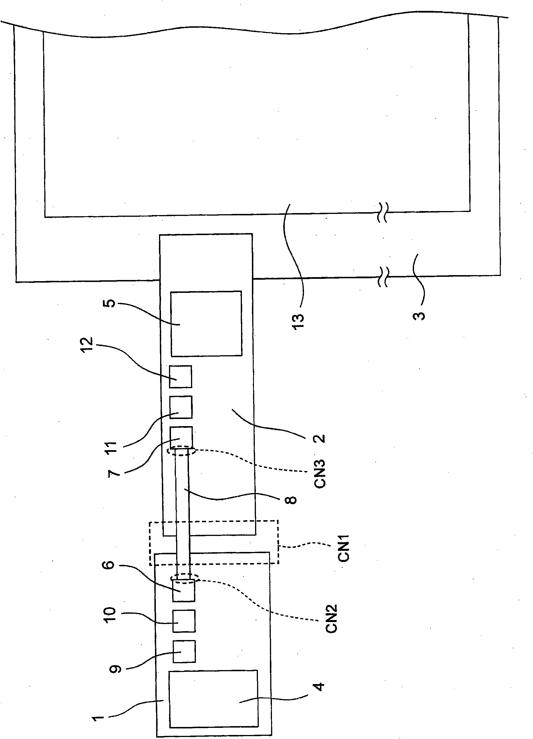
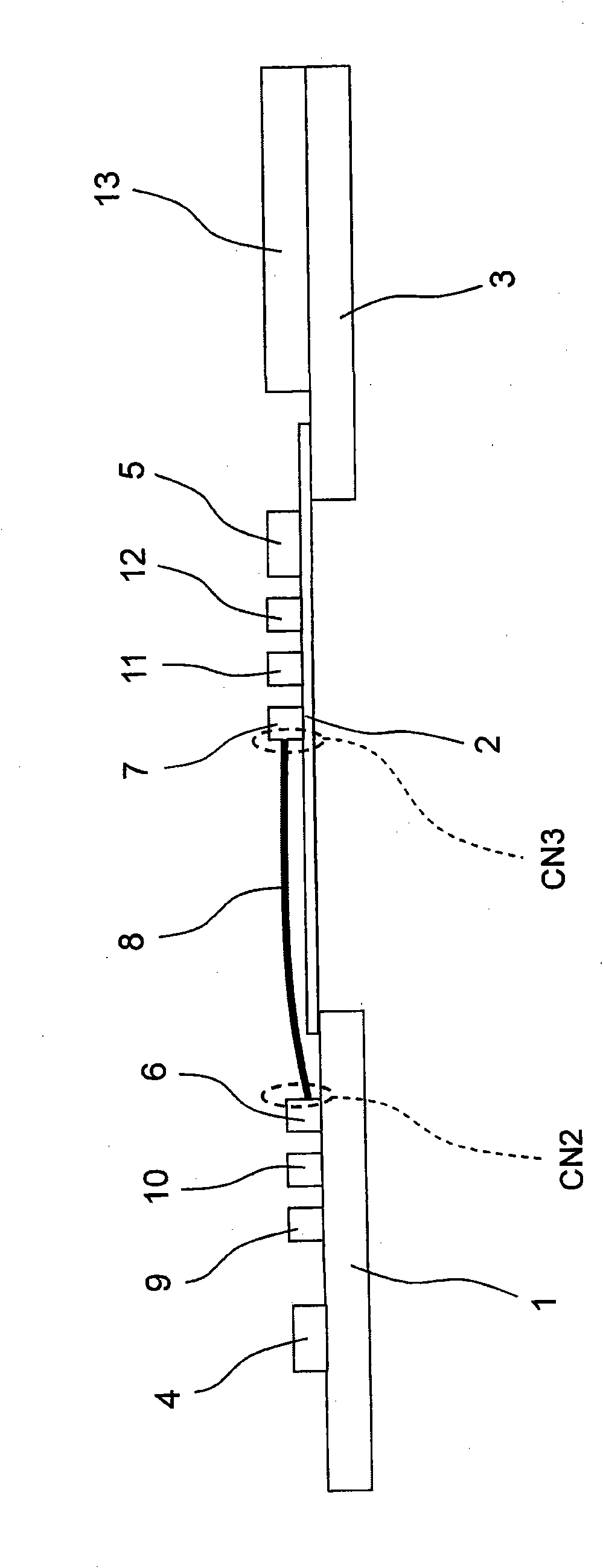
[0123] figure 1 The structure of the transmission system for the image display device of the first embodiment is schematically shown, in which the image display drive IC 5 is connected to a glass substrate as an example of a first circuit substrate mounted on the display panel 13 by a TAB method. The display panel 13 includes a substrate and a liquid crystal layer sealed between the substrate and the glass substrate 3 . Although not shown, the glass substrate 3 is provided with scanning signal lines (or data signal lines), and the substrate of the display panel 13 is provided with data lines arranged in the direction crossing the scanning signal lines (or data signal lines) of the glass substrate 3 . Signal line (or scan signal line). In addition, switching devices are connected between each signal line and each pixel electrode (not shown) arranged in a matrix shape. In addition, the inventive point of the present invention does not lie in the structure and arrangement of t...

no. 2 example

[0159] Figure 8 A transmission system for an image display device according to a second embodiment of the optical TAB method is shown. The optical transmission path is composed of an optical transmission path 8 which is an overhead wiring floating in the air, and a substrate-integrated optical transmission path 14 integrally formed with the flexible substrate 2 . The three optical connections between the light emitting device 6 and the optical transmission path 8 , the optical transmission path 8 and the substrate-integrated optical transmission path 14 , and the substrate-integrated optical transmission path 14 and the light-receiving device 7 are necessary structures. The configurations shown in FIGS. 3 to 7 can be applied to the optical connection portion CN2 between the light emitting device 6 and the optical transmission path 8 and the optical connection portion CN3 between the board-integrated optical transmission path 14 and the light receiving device 7 .

[0160] The...

no. 3 example

[0175] Figure 13 In a transmission system for an image display device showing a third embodiment of the optical TAB method, a substrate-integrated optical transmission line 14 is formed on a circuit board 1 and a flexible substrate 2 .

[0176] Such as Figure 13 As shown, the image processing IC4, SER9, driver IC10 and light emitting device 6 are installed on the circuit substrate 1. In addition, a light receiving device 7 , an amplifier IC 11 , a DES 12 , and an image display driver IC 5 are mounted on the flexible substrate 2 . The optical signal emitted by the light-emitting device 6 is transmitted in the substrate-integrated optical transmission path 14A provided on the circuit board 1, passes through the optical connection part, passes through the substrate-integrated optical transmission path 14B provided on the flexible substrate 2, and is sent to the light-receiving device. 7 receive. And, the signal which becomes an electric signal by the light receiving device 7...


PUM


Abstract

A transmission system for an image display device has a first circuit board and a second circuit board, a flexible member for connecting the first circuit board and the second circuit board, an image display driver IC mounted on the first circuit board or the flexible member, an image processing IC mounted on the second circuit board, and an optical transmission path. At least part of signals to be transmitted between the image display driver IC and the image processing IC is transmitted as an optical signal.

Description

technical field [0001] The present invention relates to a transmission system for an image display device and electronic equipment, and more particularly to a transmission system for an image display device that transmits signals between an image display driver IC and an image processing IC, and electronic equipment using the transmission system for an image display device. Background technique [0002] Regarding electronic equipment currently using a transmission system for an image display device, a liquid crystal display device, which is the most common as an image display device, will be described. [0003] In an active matrix type liquid crystal display device, an image display section is provided in which a plurality of pixels are arranged in a matrix shape. The image display unit has two substrates and liquid crystal sealed between the substrates. In order to make the liquid crystal on the pixel generate an electric field, a pixel electrode corresponding to each pixe...

Claims


Application Information

Patent Timeline
Patent Type & Authority Applications(China)
IPC IPC(8): G02F1/13G09F9/00G02F1/1345G09G3/20
CPCG02F1/13452G02B6/4212G02B6/4231G02B6/423G02B6/43
Inventor 渡边隆裕名仓和人
Owner SHARP KK
Learn More