This helps you quickly interpret patents by identifying the three key elements:
Problems solved by technology
Method used
Benefits of technology
Problems solved by technology
[0004] In the above-mentioned liquid crystal display device, as the pixel becomes more high-definition, the wiring resistance increases accordingly, so signal delay tends to occur.
Method used
Image
Click on the blue label to locate the original text in one second.
Reading with bidirectional positioning of images and text.
Examples
Embodiment approach 1
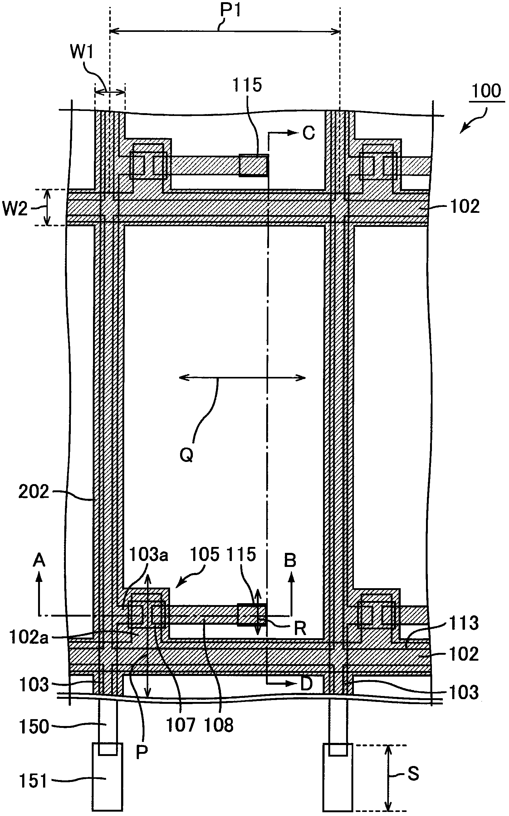
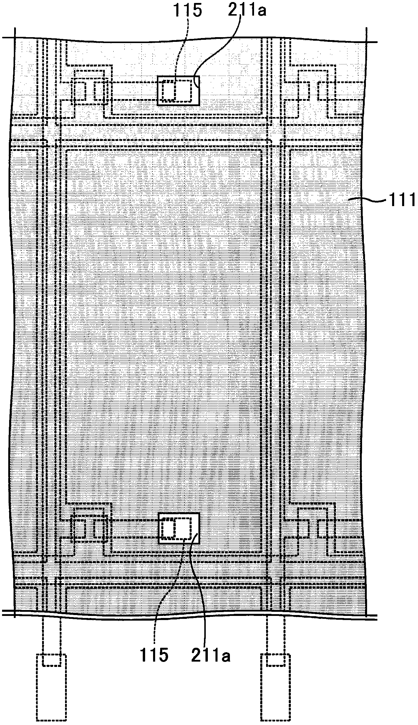
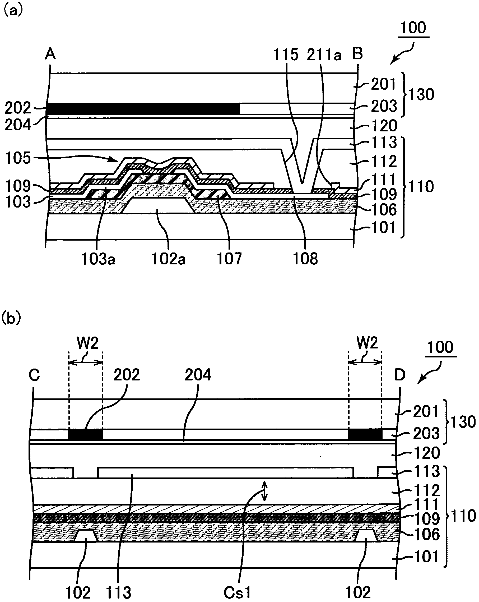
[0067] Picture 1-1 is a schematic plan view showing the configuration of a pixel of the liquid crystal display device according to Embodiment 1 of the present invention, Figure 1-2 It is a schematic plan view showing the structure of a transparent conductive film. figure 2 (a) is along Picture 1-1 A schematic cross-sectional view of the line A-B in, figure 2 (b) is along Picture 1-1 Schematic cross-sectional view of line C-D in .
[0068] exist Picture 1-1 , figure 2 In (a) and (b), the liquid crystal display device 100 includes a TFT array substrate 110 , a liquid crystal layer 120 , and a color filter (CF) substrate 130 as an opposing substrate. The TFT array substrate 110 and the CF substrate 130 are arranged facing each other with the liquid crystal layer 120 interposed therebetween.
[0069] Gate lines (scanning lines) 102 and source lines (signal lines) 103 are arranged in a grid pattern on the main surface of a support substrate 101 constituting the TFT a...
Embodiment 1
[0110] As a result of setting the pixel pitch P1 to 39 μm in the liquid crystal display device 100 of Embodiment 1, even with the same pixel size, it is comparable to a liquid crystal display device formed by a process using five normal masks (comparative implementation described later). Compared with the liquid crystal display device 500 of Embodiment 1, the aperture ratio is increased by 35%.
[0111] In the present invention, if a sufficient storage capacitance cannot be secured with the configuration of the first embodiment, the aperture ratio of the pixel will be slightly lowered. However, Cs wiring and Cs electrodes may be provided to ensure storage capacitance. Next, a configuration in which Cs wiring and / or Cs electrodes are provided will be described.
Embodiment approach 2
[0113] In this embodiment, an example in which a Cs electrode is provided in addition to the configuration of Embodiment 1 to ensure storage capacitance will be described. Components having the same configuration as those in the first embodiment described above are denoted by the same reference numerals and description thereof will be omitted.
[0114] Figure 5-1 is a schematic plan view showing the configuration of a pixel of a liquid crystal display device according to Embodiment 2 of the present invention, Figure 5-2 It is a schematic plan view showing the structure of a transparent conductive film. Figure 6 (a) is along Figure 5-1 A schematic cross-sectional view of the line A-B in, Figure 6 (b) is along Figure 5-1 The schematic cross-section of line C-D in, Figure 6 (c) is shown Figure 6 An enlarged schematic view of a part of (b).
[0115] exist Figure 5-1 In the liquid crystal display device 210, the TFT 105 is located at the lower left corner of the pi...
PUM
Property
Measurement
Unit
viewing angle
aaaaa
aaaaa
coating thickness
aaaaa
aaaaa
Abstract
The present invention provides a liquid crystal display device and a method for manufacturing the same that can improve aperture ratio of pixels while securing necessary storage capacitance using a simple configuration even if there is progress in high resolution of pixels. The liquid crystal display device according to the present invention is provided with a plurality of pixels. A thin film transistor array substrate includes gate lines and source lines arranged in a grid pattern on a principal surface of a supporting substrate, transparent pixel electrodes, and thin film transistors. Also, the thin film transistor array substrate includes a gate insulator, a passivation layer, a transparent conductive film, a first insulation layer, and transparent pixel electrodes stacked in order from a supporting substrate side. The transparent pixel electrodes are electrically connected with drain electrodes of the thin film transistors through contact holes formed in the first insulation layer. When a substrate surface is viewed in a direction of a normal to the substrate surface, the transparent conductive film does not overlap regions in which the transparent pixel electrodes and the drain electrodes are electrically connected with each other.
Description
technical field [0001] The present invention relates to a liquid crystal display device and a manufacturing method thereof. In more detail, it relates to an active matrix type liquid crystal display device and a manufacturing method thereof. Background technique [0002] In the field of display devices such as liquid crystal display devices and organic EL displays, high-definition pixels are being advanced in response to demands for improvement in resolution and miniaturization of devices. In addition, not only high-definition pixels are required, but also high aperture ratios of pixels are required. These requirements are particularly prominent in a high-definition liquid crystal display device with a pixel pitch of 40 μm or less. [0003] For example, Patent Document 1 proposes an active-matrix liquid crystal display device that realizes high-definition pixels. An active matrix liquid crystal display device has a configuration in which a liquid crystal layer is disposed...
Claims
Application Information
Patent Timeline
Application Date:The date an application was filed.
Publication Date:The date a patent or application was officially published.
First Publication Date:The earliest publication date of a patent with the same application number.
Issue Date:Publication date of the patent grant document.
PCT Entry Date:The Entry date of PCT National Phase.
Estimated Expiry Date:The statutory expiry date of a patent right according to the Patent Law, and it is the longest term of protection that the patent right can achieve without the termination of the patent right due to other reasons(Term extension factor has been taken into account ).
Invalid Date:Actual expiry date is based on effective date or publication date of legal transaction data of invalid patent.

