Semiconductor chip package and quad flat non-pin package

A technology of leadless packaging and chip packaging, which is applied in the direction of semiconductor devices, semiconductor/solid-state device parts, electric solid-state devices, etc., can solve the problem of high cost and achieve the effect of cost reduction

Inactive Publication Date: 2010-11-17
MEDIATEK INC
View PDF0 Cites 3 Cited by
  • Summary
  • Abstract
  • Description
  • Claims
  • Application Information

AI Technical Summary

Problems solved by technology

Typically a PCB with a 3mil wire width costs about 5%-10% more than a PCB with a 4mil wire width

Method used


Image

  • Semiconductor chip package and quad flat non-pin package
  • Semiconductor chip package and quad flat non-pin package
  • Semiconductor chip package and quad flat non-pin package

Examples


Embodiment Construction

[0023] In order to make the above and other objects, features, and advantages of the present invention more obvious and understandable, the following specifically enumerates the preferred embodiments with accompanying drawings, which are described in detail as follows. It should be noted that the following embodiments are only used to illustrate the purpose of the present invention, and are not a limitation of the present invention. The scope of rights of the present invention shall be subject to the claims.

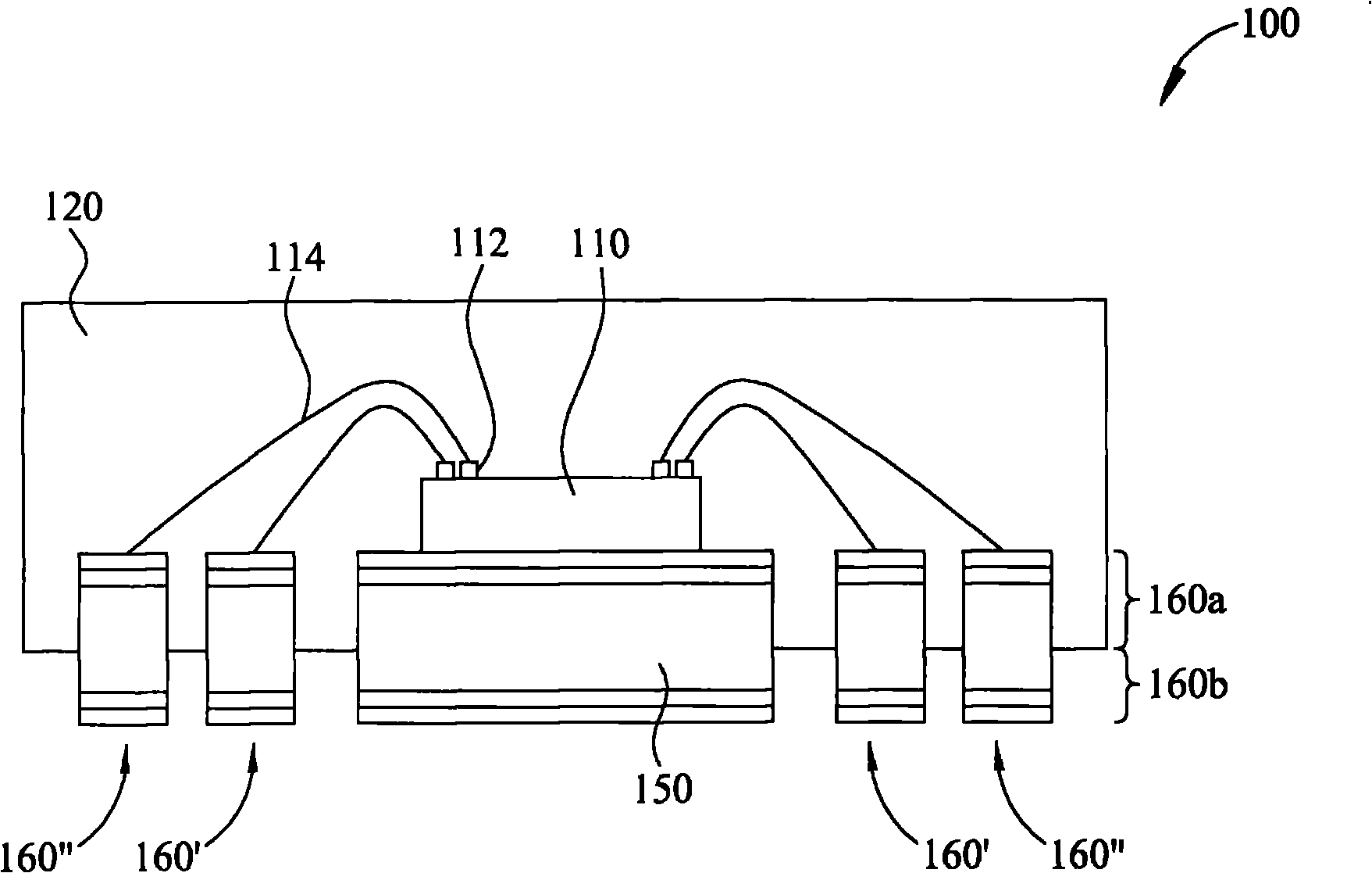
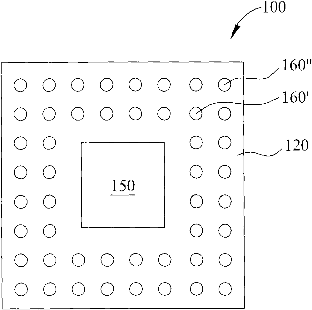
[0024] Figure 4 It is a cross-sectional view of a QFN package 200 according to an embodiment of the present invention. Figure 5 for Figure 4 The bottom view of the QFN package 200 shown. Such as Figure 4 with Figure 5 As shown, the QFN package 200 includes a chip 210 attached to a bare chip pad 250; a plurality of internal connection pads 260 are arranged around the periphery of the bare chip pad 250; and a plurality of middle connection pads 260 ', are arranged aroun...


PUM


Abstract

The invention relates to a semiconductor chip package and quad flat non-pin package. The quad flat non-pin package includes a chip, a plurality of first and second connection pads, a plurality of bonding pads and a packaging body. The first and second connection pads have different bottom surface shapes when viewed from a bottom of the quad flat non-pin package; bonding pads are provided on an active surface of the chip and are electrically connected with corresponding first and second connection pads through bonding wires; and a package body encapsulating the chip, the bonding wires and an upper portion of each of the first and second connection pads such that a lower portion of each of the first and second connection pads extends outward from a bottom of the package body. The semiconductor chip package and quad flat no-lead package can be used for PCB with larger wire width, and can reduce PCB costs.

Description

Technical field [0001] The present invention relates to semiconductor chip packaging and quad flat no-lead packaging. Background technique [0002] Low-pin-count chip package (low-pin-count chip package) is popular because of its low price, and because the cost of low-pin-count chip package is lower than that of thin and fine pitch ball grid array (Thin and Fine pitch Ball Grid Array, TFBGA) and widely used in this industry. [0003] With the accelerated improvement of semiconductor technology, operation speed and corresponding design complexity continue to increase. In response to the need for improved semiconductor technology, efficient semiconductor packaging technology, such as high-density packaging, is required. Quad Flat Non-lead (Quad Flat Non-lead, hereinafter referred to as QFN) package is a popular low-pin-count high-density package type. Because QFN packages have relatively short signal traces and faster signal transmission speeds, QFN packages have become the mainst...

Claims


Application Information

Patent Timeline
Patent Type & Authority Applications(China)
IPC IPC(8): H01L23/13H01L23/492
CPCH01L2924/01015H01L2224/484H01L24/48H01L2924/01046H01L24/45H01L2924/01082H01L2224/48599H01L23/3107H01L2924/01079H01L2224/48247H01L23/49541H01L2924/01005H01L2924/01033H01L2924/01006H01L23/49582H01L2224/85464H01L2924/01074H01L2924/01028H01L2224/45144H01L2224/85444H01L2224/48091H01L2924/014H01L2224/48644H01L2224/48664H01L2924/181H01L2924/00014H01L2924/00H01L2924/00012
Inventor 张峻玮谢东宪刘嘉惠
Owner MEDIATEK INC
Why Eureka
Try Eureka