Electro-optical panel, electro-optical device, and electronic apparatus

a technology of electrooptical devices and electronic devices, applied in the direction of identification means, electrical apparatus casings/cabinets/drawers, display/control units, etc., can solve the problems of high-performance ic development, heat generation problems, and difficulty in ensuring a sufficient terminal arrangement area, etc., and achieve the effect of small siz

Active Publication Date: 2018-08-09
SEIKO EPSON CORP
View PDF7 Cites 4 Cited by
  • Summary
  • Abstract
  • Description
  • Claims
  • Application Information

AI Technical Summary

Benefits of technology

[0004]An advantage of some aspects of the invention is to provide a technique capable of realizing an electr

Problems solved by technology

If the number of pixels is increased to realize a high resolution, since there is an increase in the number of panel terminals such as a terminal to which a signal that controls the display of each pixel is applied, it is difficult to ensure a sufficient terminal arrangement area.
However, development of a high-performance IC is costly, for example, and problems of heat generation also occur.
However, as the size of the panel continues to decrease, it may be difficult to ensure a terminal mounting area ev

Method used


Image

  • Electro-optical panel, electro-optical device, and electronic apparatus
  • Electro-optical panel, electro-optical device, and electronic apparatus
  • Electro-optical panel, electro-optical device, and electronic apparatus

Examples


first embodiment

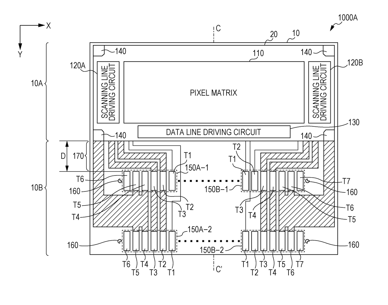
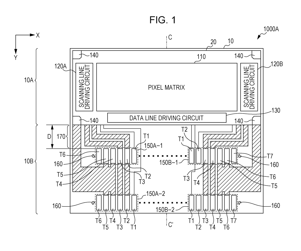
[0026]FIG. 1 is a plan view of an electro-optical panel 1000A according to an embodiment of the invention. The electro-optical panel 1000A is an active matrix-type liquid crystal display device for a display unit of an electronic apparatus which is small in size such as a projection-type projector. The electro-optical panel 1000A includes an element substrate 10 (a semiconductor substrate on which a semiconductor is formed, or simply a substrate) and a counter substrate 20. The element substrate 10 has a rectangular planar shape, and a surface of the element substrate 10 is divided into a first area 10A and a second area 10B each of which has a rectangular planar shape. The counter substrate 20 has a rectangular planar shape slightly smaller than the first area 10A and is mounted on the first area 10A. Hereinafter, as illustrated in FIG. 1, a transverse direction (first direction) of the first area 10A is referred to as the Y direction, and a longitudinal direction (second direction...

second embodiment

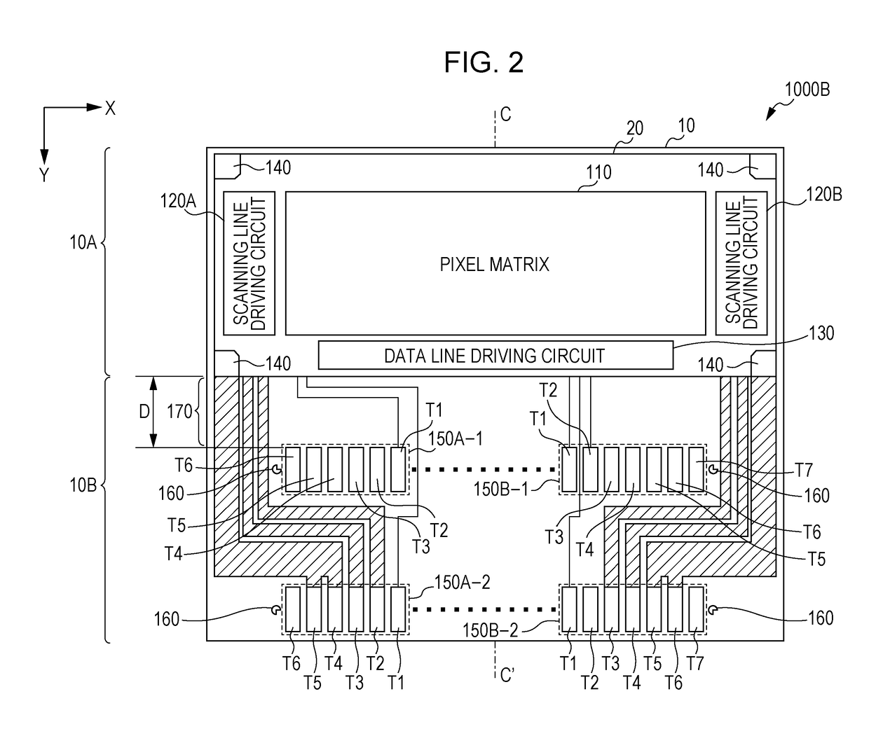
[0038]FIG. 2 is a plan view of an electro-optical panel 1000B according to a second embodiment of the invention. In FIG. 2, the same components as those in FIG. 1 are denoted by the same reference numerals. As is apparent from a comparison between FIG. 2 and FIG. 1, the electro-optical panel 1000B according to the second embodiment is different from the electro-optical panel 1000A according to the first embodiment in that terminals T2 to T5 of six terminals arranged in the terminal area 150A-1 are dummy terminals and terminals T3 to T7 of seven terminals arranged in the terminal area 150B-1 are dummy terminals.

[0039]The roles of the terminal T1 arranged in the terminal area 150A-1 and the terminals T1 to T6 arranged in the terminal area 150A-2 are the same as those of the first embodiment. The roles of the terminals T1 and T2 arranged in the terminal area 150B-1 and the terminals T1 to T7 arranged in the terminal area 150A-2 are the same as those of the first embodiment. As illustra...

third embodiment

[0041]FIG. 3 is a plan view of an electro-optical panel 1000C according to a third embodiment of the invention. In FIG. 3, the same components as those in FIG. 1 are denoted by the same reference numerals. The roles of the terminals T1, T2, and T6 in the terminal area 150A-1 and the roles of the terminals T1 to T6 in the terminal area 150A-2 of the third embodiment are the same as those of the first embodiment, whereas the roles of the terminals T3 to T5 in the terminal area 150A-1 are different from those of the first embodiment. Similarly, the roles of the terminals T1 to T3 and T7 in the terminal area 150B-1 and the roles of the terminals T1 to T7 in the terminal area 150B-2 are the same as those of the first embodiment, whereas the roles of the terminals T4 to T6 in the terminal area 150B-1 are different from those of the first embodiment.

[0042]More specifically, in the terminal area 150A-1, the low potential side power supply line voltage VSS is applied to the terminal T3, and ...


PUM


Abstract

Provided is an electro-optical panel including a first area in which a circuit is formed and a first terminal area and a second terminal area that are arranged side-by-side in a Y direction when viewed from the first area. The first terminal area and the second terminal area are each provided with a terminal group including a plurality of terminals arranged in an X direction different from the Y direction, and at least one of wires from the first terminal area to the first area and from the second terminal area to the first area extends from between the first terminal area and the second terminal area and reaches the first area through an area outside of the first terminal area when viewed from a central axis of the electro-optical panel extending in the Y direction.

Description

BACKGROUND1. Technical Field[0001]The present invention relates to an electro-optical panel which is small in size and capable of performing a high-resolution display, an electro-optical device, and an electronic apparatus.2. Related Art[0002]High resolution properties and miniaturization of an electro-optical device such as a liquid crystal panel (liquid crystal light valve) usable for a liquid crystal projector are in progress. If the number of pixels is increased to realize a high resolution, since there is an increase in the number of panel terminals such as a terminal to which a signal that controls the display of each pixel is applied, it is difficult to ensure a sufficient terminal arrangement area. In addition, when the number of pixels is increased to realize a high resolution, the load of the driving circuit that drives each pixel is increased accordingly, and therefore there is a need to use an integrated circuit (IC) with a high performance to constitute the driving circ...

Claims


Application Information

Patent Timeline
IPC IPC(8): H05K5/00H05K1/02H05K1/11
CPCH05K5/0017H05K1/0274H05K1/11H05K1/0296H05K2201/09918G09F9/35G02F1/13452H05K1/189H05K3/323H05K2201/10128H05K2201/10136
Inventor FUJIKAWA, SHINSUKE
Owner SEIKO EPSON CORP
Why Eureka
Try Eureka